You are viewing the documentation for an older COMSOL version. The latest version is
available here.
The Optical Transitions feature is designed to model optical absorption and stimulated and spontaneous emission within the semiconductor. Stimulated emission or absorption occurs when a transition takes place between two quantum states in the presence of an oscillating electric field, typically produced by a propagating electromagnetic wave. For a semiconductor the process of stimulated absorption occurs when an electron in the valence band adsorbs a photon and transitions into the conduction band (resulting in coherent absorption of light). Stimulated emission occurs when an electron in the conduction band is stimulated by the field to transition down to the valence band (resulting in coherent emission of light). Spontaneous emission occurs when transitions from a high energy to a lower energy quantum state occur, with the emission of light. It can be regarded as a process by which a system returns to equilibrium, and correspondingly can be linked to the stimulated emission in equilibrium by thermodynamic arguments. Spontaneous emission does not occur in phase with any propagating waves in the system, and indeed can occur in the absence of such waves. Currently the optical transitions feature is dedicated to treating both stimulated and spontaneous emission in
direct band gap semiconductors. Consequently the theory in the subsequent sections assumes a direct band gap at several points.
where A is the magnetic vector potential and
m0 is the electron mass (
not the effective mass).
For most practical optical applications |qA|
« |
p| (
Ref. 34) so the
q2A⋅A term can be neglected. When modeling electromagnetic fields in the frequency domain, COMSOL employs a gauge that ensures that the time varying electric potential is zero and the magnetic potential satisfies the equation
∇⋅A=0 (see
Magnetic and Electric Potentials in the
COMSOL Multiphysics Reference Manual for further details on gauge fixing for electromagnetic waves). With this gauge for
A the

term is zero. Consequently the quantum mechanical Hamiltonian operator takes the form:
Since |qA|
« |
p| the time-dependent term that includes the vector potential can be treated as a small perturbation to the original stationary Hamiltonian
H0 such that:
(3-99)

(3-100)

Equation 3-99 is the Hamiltonian for the semiconductor in the absence of the field, which has eigenfunctions of the form given in
Equation 3-14.
Since the change to the electron Hamiltonian is small, time-dependent perturbation theory can be used to solve the problem (see Ref. 8 for an introduction to time-dependent perturbation theory that derives the main results used below). For small, oscillatory perturbations to a stationary Hamiltonian, a key result of time dependent perturbation theory (known as Fermi’s golden rule) predicts that the probability of a transition from an occupied state (1) to an unoccupied state (2, in this case at a higher energy than state 1) per unit time,
W1→2 is given by:
(3-101)

where E1 and
E2 are the corresponding eigenvalues of the states,
ω0 is the angular frequency of the oscillation and
H12' is the matrix element corresponding to the oscillatory perturbation (
H') to the original Hamiltonian:
Equation 3-101 gives the transition probability between two discrete states. The delta function indicates that the states must be separated by an energy equal to the photon energy, that is the transition must conserve energy. An additional requirement on the transition is that crystal momentum is conserved:
(3-102)

where kopt is the photon wave vector. This requirement for crystal momentum conservation can be derived using a periodic expansion of the Bloch functions for the two wave functions in the matrix element
H12' with a plane wave excitation (see, for example,
Ref. 34 and
Ref. 35). However, the relation is in practice much more general since it results from fundamental symmetries of the system Hamiltonian (see Appendix M of
Ref. 1). Typical optical wavelengths (400 to 700 nm in free space, dropping by a factor of order 10 inside the semiconductor) are significantly larger than the unit cell size of a semiconductor (typically less than 1 nm), which in turn determines the order of the Bloch function wavelengths. Consequently
kopt is usually neglected in
Equation 3-99 leading to
k2 = k1.
Equation 3-101 describes the transition rate from an unoccupied initial state to an occupied final state. To obtain the net rate of stimulated emission (including both upward and downward transitions) it is necessary to sum over all transitions from occupied to unoccupied states.
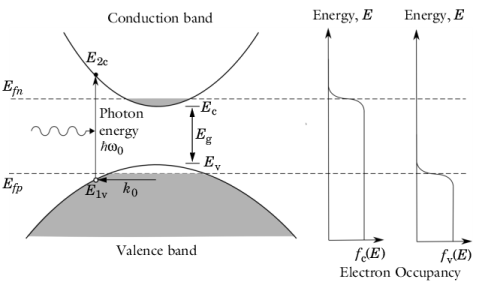
Figure 3-11 shows the transitions of interest in a simple two-band model. Due to the spherical symmetry of the constant energy surfaces in
k-space (in a direct band-gap semiconductor), upward transitions occur between states of fixed energy in the valence band (
E1v) and in the conduction band (
E2c).
Assuming that the bands have a parabolic dispersion relation in the vicinity of k = 0,
E1v and
E2c can be written as a function of the photon energy,

. The equations:
can be rearranged into the form of a single quadratic equation for k0. The equation has a single physically significant root (for positive
k):
(3-103)

For states with a given magnitude of k we can define an average matrix element

which represents the averaged matrix element over all directions for a given excitation. For unpolarized light the random orientation of the polarization can also be accounted for in

(note that usually in the literature unpolarized light is assumed, and matrix elements quoted should be adjusted if polarized light is under consideration). Note also that the matrix element is in general a function of the magnitude of
k, but for small values of
k the assumption is generally made that it is independent of
k.
(3-104)

Equation 3-104 is the equation for the transition rate between a single pair of states. In a semiconductor, there are many states that satisfy
Equation 3-103, and correspondingly it is necessary to integrate over pairs of states for which the transition can occur. Clearly an upward transition must take place from a full state into an empty state, so the occupancy of the states must also be accounted for. One of the assumptions underlying the drift diffusion equations is that the scattering within the band occurs on a much smaller time scale than equilibrating processes that occur between the bands. Consequently stimulated electrons can be considered to equilibrate rapidly within the conduction band so that their distribution is described by the Fermi-Dirac function with the appropriate electron quasi-Fermi level. Correspondingly, the rate of stimulated absorption (the total number of upward transitions per unit volume per unit time, SI unit: m
-3s
-1) is given by:
(3-105)

where g(
k) is the density of states in k-space (1/4
π3 from
Equation 3-19) and the
electron occupancy factors for the conduction and valence band,
fc and
fv, are given by:
(3-106)

E2c and
E1v can be written in terms of
k, leading to the equation:
Note that Equation 3-103 was used in the third and fourth steps. It is common to rewrite this expression in the form:
(3-107)

is defined by analogy with Equation 3-21 and where the functional dependence of
fc and
fv has been dropped.
The rate of stimulated absorption is directly related to the rate of stimulated and spontaneous emission as a result of physical and thermodynamic arguments originally due to Albert Einstein (Ref. 36). Historically Einstein argued for the existence of stimulated emission by means of an argument similar to the one presented here. In the argument that follows the existence of stimulated emission is assumed from the outset.
(3-108)

where B12 and
B21 represent constants related to the semiconductor material and

is the mean number of photons per unit volume per unit photon energy (SI unit: J
−1m
−3).
(3-109)

where A21 is another constant. When the semiconductor is in equilibrium with the radiation field the two quasi-Fermi levels are equal and the emission and absorption rates must balance. Consequently, for the equilibrium case:
(3-110)

(3-111)

(3-112)

The form of Equation 3-112 is similar to that of the Planck blackbody radiation spectrum, which is observed to hold experimentally for many materials (for example, see
Ref. 10 §63 or
Ref. 34 section 9.2.1):
(3-113)

where the relation  is used. Equation 3-111
 and
Equation 3-113 are derived assuming an exciting field with a distributed spectrum in thermal equilibrium. However the phenomenological models described by
Equation 3-108 and
Equation 3-109 are expected to apply away from equilibrium in the same form, so the relationships between
A21,
B12, and
B21 are general.
Equation 3-113, which describes spontaneous emission relates to a process that is entirely independent of the exciting radiation. Correspondingly,
A21 = 1/τspon is written, which allows the phenomenological equations to be written in the following form:
(3-114)

These relationships apply for a distributed spectrum of incident radiation. In order to relate the present analysis to that in the preceding section, consider how to relate the case of a monochromatic field to that of a distributed spectrum, with a spectral width that is large compared to the transition width. One way this can be done is to consider the process of building up the distributed absorption rate

from the absorption rates due to a series of monochromatic fields, with appropriately scaled energy densities (
Ref. 37). For some coefficient
C, a single, monochromatic line spectrum at frequency
ω0 leads to the following frequency domain contribution to the rate of stimulated generation:

where nE (SI unit: m
-3) is the photon density at the photon energy
 .
. To build up the corresponding distributed spectrum requires summing over a series of these line spectra, each with a different value for the driving photon energy
E’ and with,
nE' = n(
E’)d(
E’). Correspondingly the sum can be transformed to an integral in the following way:
(3-115)

(3-116)

(3-117)

Note that fc and
fv are both functions of
E through
Equation 3-106 and
Equation 3-103.
Equation 3-116 and
Equation 3-117 determine the rates of stimulated and spontaneous emission in terms of the spontaneous lifetime. The spontaneous lifetime can be related to the matrix element for the transition, discussed in the previous section. The energy density of the electromagnetic field for a traveling wave in a dielectric medium is
ε0εr′E02/2 where
E0 is the electric field norm and
εr′ is the real part of the medium permittivity. Correspondingly the number density of the photons is given by:
Comparing this equation with Equation 3-107 shows that the following relationship exists between the matrix element and the spontaneous emission lifetime:
(3-118)

As a result of Equation 3-118 the rates of spontaneous and stimulated emission can also be written in the form:
(3-119)

Equation 3-100 showed the perturbation to the electric field could be written in the form:
The matrix element in this form depends on the magnitude of the magnetic vector potential. It is often more convenient to express the matrix element in terms of the amplitude of the electric field oscillation (E0) and a unit vector in the direction of the electric field (
e). With the frequency domain gauge for the oscillatory field in COMSOL Multiphysics, the electric field is related to the magnetic field by the equation:
Consequently Equation 3-100 can be written in the form:
(3-120)

The momentum matrix element between to states 1 and 2 (<2|e⋅p|1> using the bracket notation) is frequently referred to in the literature as M
12 — a convention adopted by COMSOL Multiphysics.
where μ is the dipole matrix element (
μ=qr where
r is the position vector) and correspondingly:
(3-121)

The matrix element <2|e⋅μ|1> is written in the form
μ12 in the user interface.
The two forms of the matrix element given in Equation 3-120 and
Equation 3-121 can be used to specify the matrix element in COMSOL Multiphysics. Note that the band averaged matrix element for the particular electric field orientation should be used (

or

). As discussed in
Ref. 38 and
Ref. 40, the band-averaged matrix elements can be derived using a
k⋅p perturbation method. For a simple 4-band model (
Ref. 38), assuming unpolarized incident light, the matrix element takes the form (
Ref. 39):
where Eg is the gap energy and
Δ is the spin orbital splitting energy of the valence band.
m* is the effective mass of electrons in the conduction band, but typically an experimentally determined value should be used rather than the theoretical value (see discussion in
Ref. 39; for the case of GaAs,
Ref. 40 provides values for other materials).
(3-122)

Here E is the electric field,
H is the magnetic field strength,
P is the material polarization,
M is its magnetization, and
V is an enclosed volume within the material, with surface
S.
Each of the terms in Equation 3-122 has a physical interpretation that can be associated with the flow of energy through the volume. The
E×H term on the left hand side of this equation describes the flow of energy out of the enclosed volume (
E×H is known as Poynting’s vector). The
E⋅j term represents the energy expended on moving charges within the volume. The next term represents the rate of change of the stored electromagnetic energy in the vacuum and the final two terms represent the power per unit volume expended on the electric and magnetic dipoles present in the material.
For optical frequencies, the E⋅j term is of order
ρE2 for a material resistivity
ρ (for heavily doped silicon
ρ is of order 10
−5 Ω/m). Most practical semiconductors are nonmagnetic, so the final term is usually not significant. In the frequency domain, the term involving the polarization is of order
ωε0E2 (
ω is of order 10
15 rad/s for optical light,
ε0 is 8.85·10
-12 F/m so
ωε0 is of order 10
4 Ω/m). Consequently, when considering the interaction of semiconductors with propagating electromagnetic waves it is only necessary to consider the material polarization. In the frequency domain, power per unit volume lost to the material is given by the term:
where χ is the (complex) material susceptibility, with real part
χ′ and imaginary part
χ″. In the frequency domain
E(
r,t) and
P(
r,t) take the form:
For an isotropic material χ becomes a scalar value:
(3-123)

Equation 3-123 shows how the imaginary part of the susceptibility is related to the power absorption by the material. Since each photon carries an energy

the total power adsorbed is directly related to the net rate of stimulated emission (given by
Equation 3-119).
(3-124)

where the superscript 0 has been added to fv,
fc, and
gred to indicate that these quantities are evaluated at the energy

which corresponds to the excitation frequency.
Equation 3-124 shows how the imaginary part of the susceptibility is related to the rate of stimulated emission and correspondingly to the transition matrix element. Associated with the change in the imaginary part of the susceptibility is a small change in the real part. If the complete frequency spectrum of the susceptibility is known, it is possible to relate the imaginary part of the susceptibility to the real part using the Kramers-Kronig relations. The Kramers-Kronig relations result from the constraint that in the time domain, the equations for the susceptibility at time
t can only depend on the electric field at times less than
t (
Ref. 41); that is, the equations are derived from considering the system to be causal. Alternatively, the equations can be derived by considering the analytic nature of the complex function
χ for physical systems (see
Ref. 34 or
Ref. 35 for derivations of this form). The Kramers-Kronig relation for the susceptibility can be written in the form:
(3-125)

Where the P indicates that the principle value of the integral is required.
Equation 3-125 gives the real part of the susceptibility in terms of the imaginary part, provided that the entire frequency spectrum of the imaginary part is known. In practice it is not possible to determine the entire frequency spectrum of the imaginary part of the susceptibility, so instead a change in the imaginary part of the susceptibility is considered due to the rearrangement of the carriers in the band. Taking as a reference configuration for the semiconductor the case of an undoped semiconductor at equilibrium (at temperatures such that the occupancy of the conduction band is negligible) we define:
(3-126)

Equation 3-126 corresponds to a reference configuration in which the semiconductor has an empty conduction band and a full valence band. The real part of the susceptibility for the reference material can then be written as:
(3-127)

where the subscript ref indicates a change from the reference configuration and where:
(3-128)

The χ0 terms can be eliminated using
Equation 3-127 giving:
(3-129)

Equation 3-129 gives the change in the real part of the susceptibility from the reference material susceptibility, for a given carrier concentration. This makes the integral easier to perform in practice, since the changes in the susceptibility due to the carriers is small at energies far from the band gap.
Equation 3-129 can be used to compute the change in the real part of the susceptibility, given a knowledge of the susceptibility of the reference material. In COMSOL Multiphysics, the real part of the susceptibility of the reference material is treated as a user-specified material property (it is determined from the relative permittivity or refractive index). The change in the refractive index due to the excitation of carriers into the valence band (either as a result of doping or due to carrier injection) is then accounted for by means of
Equation 3-129. Note that
χref′′(
ω) is
not known over all frequencies and the real part of the susceptibility is likely to have significant contributions from other processes that occur at frequencies away from those corresponding to the band gap. However, since it is possible to define
Δrefχ′′(
ω) from
Equation 3-128 we can compute the change in the real part of the susceptibility from
Equation 3-129.
At the excitation frequency, ω0, the imaginary part of the susceptibility due to optical transitions can be computed directly from
Equation 3-126. Since the imaginary part of the reference material susceptibility is not conveniently available as a material property, COMSOL Multiphysics calculates this part of the susceptibility directly. It is possible to include additional contributions to the imaginary part of the susceptibility from mechanisms other than the optical transitions, as discussed in the next section.
The results from the preceding section have been used in deriving the above equations. Note that for the real part of the permittivity, the initial permittivity value is the real part of the permittivity for the reference material at the excitation frequency (χ′ref(
ω0)), and the change in the permittivity is the same as
Δrefχ′(
ω0). However, this is
not the case for the imaginary part of the susceptibility, because the reference material contribution to the imaginary part of the permittivity is not generally available as a a material property. The change in the imaginary part of the permittivity is given by:

Typically the initial value of the imaginary part of the permittivity (εr,i′′) is zero. COMSOL Multiphysics allows for nonzero values of
εr,i′′ for cases in which there are other loss mechanisms in the material besides the optical transitions, so it is possible to enter nonzero values for this parameter in the feature. These mechanisms contribute in an additive manner to the material losses (or gain). The change in the imaginary part of the permittivity is given by:
where χ′′(
ω0) is given by
Equation 3-124.
In optical applications it is often more common to specify the real and imaginary parts of the refractive index (n-i
k) than to specify the complex relative permittivity. Simple relationships exist relating these quantities, allowing the material properties to be expressed in either form. In general, the complex permittivity is equal to the square of the complex refractive index (see
Ref. 34,
Ref. 35, or
Ref. 37), so that:
In practical semiconducting materials, ki,
Δk, and
Δn are small in comparison to
ni, so the terms in the square brackets are small. This is assumed when generating the corresponding postprocessing variables.