Tutorial Model: DC Characteristics of a MOSFET
This tutorial calculates the DC characteristics of a MOS (metal-oxide semiconductor) transistor. The MOSFET (metal oxide semiconductor field-effect transistor) is by far the most common semiconductor device, and the primary building block in all commercial processors, memories, and digital integrated circuits. Since the first microprocessors were introduced approximately 40 years ago this device has experienced tremendous development, and today it is being manufactured with feature sizes of 22 nm and smaller.
The MOSFET is essentially a miniaturized switch. In this example the source and drain contacts (the input and output of the switch) are both ohmic (low resistance) contacts to heavily doped n-type regions of the device. Between these two contacts is a region of p-type semiconductor. The gate contact lies above the p-type semiconductor, slightly overlapping the two n-type regions. It is separated from the semiconductor by a thin layer of Silicon oxide, so that it forms a capacitor with the underlying semiconductor. Applying a voltage to the gate changes the local band structure beneath it through the Field Effect. A sufficiently high voltage can cause the semiconductor to change from p-type to n-type in a thin layer (the channel) underneath the gate. This is known as inversion and the channel is sometimes referred to as the inversion layer. The channel connects the two n-type regions of semiconductor with a thin n-type region under the gate. This region has a significantly lower resistance than the series resistance of the n-p/p-n junctions that separated the source and the drain before the gate voltage produced the inversion layer. Consequently, applying a gate voltage can be used to change the resistance of the device. The gate voltage where a significant current begins to flow is called the threshold or turn-on voltage. Figure 7 shows a schematic MOSFET with the main electrical connections highlighted. Figure 8 shows an electron microscope image of a modern MOSFET device.
Figure 7: Schematic diagram of a typical MOSFET. The current flows from the source to the drain through a channel underneath the gate. The size of the channel is controlled by the gate voltage.
Figure 8: Cross-section TEM (transmission electron microscopy) image of a 50 nm gate length MOSFET fabricated at KTH Electrum laboratory by P.E Hellström and coworkers within the ERC advanced grant OSIRIS research project headed by Prof. M. Östling.
As the voltage between the drain and the source is increased the current carried by the channel eventually saturates through a process known as pinch-off, in which the channel narrows at one end due to the effect of the field parallel to the surface. The channel width is controlled by the gate voltage. Typically a larger gate voltage results in wider channel and consequently a lower resistance for a given drain voltage. Additionally, the saturation current is larger for a higher gate voltage.
Figure 9: Model geometry showing the external connections.
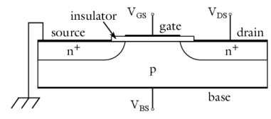
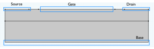
Figure 9 shows the model geometry, indicating how the geometry elements correspond to features in Figure 7. In this model both the source and the base are connected to ground and the voltages applied to the drain and the gate are varied. In the first study a small voltage (10 mV) is applied to the Drain and the Gate voltage is swept from 0 to 5 V. A plot of the current flowing between the source and the drain is used to determine the turn-on voltage of the device. The second study sweeps the drain voltage from 0 to 5 V at three different values of the gate voltage (2, 3 and 4 V). The drain current versus drain voltage is then plotted at several values of the gate voltage.