|
|
|
|
1
|
|
2
|
|
3
|
Click Add.
|
|
4
|
Click
|
|
5
|
|
6
|
Click
|
|
1
|
|
2
|
|
1
|
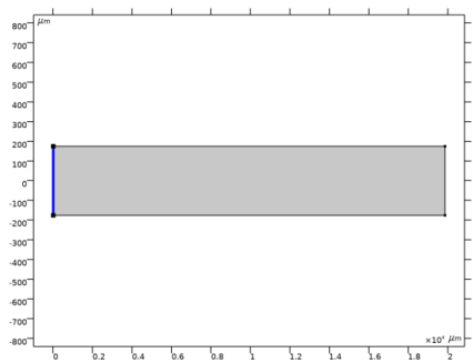
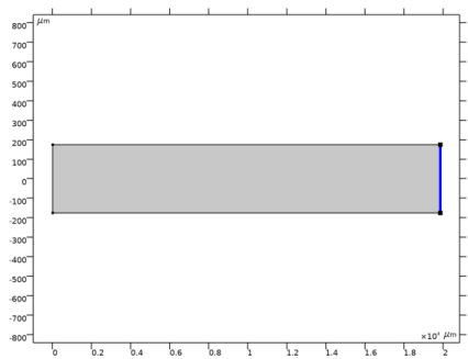
In the Model Builder window, expand the Component 1 (comp1)>Definitions>View 1 node, then click Axis.
|
|
2
|
|
3
|
|
4
|
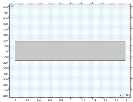
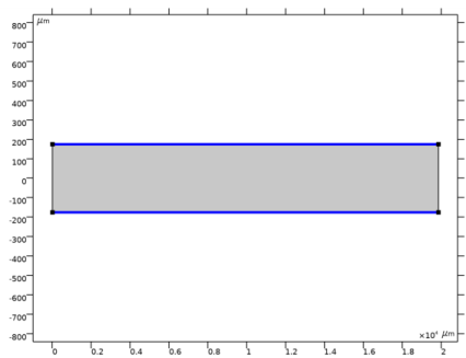
In the y scale text field, type 10, to make the view of the waveguide less wide. Notice though that the propagation angle now looks much steeper.
|
|
1
|
|
2
|
|
3
|
|
4
|
|
5
|
|
6
|
|
7
|
|
8
|
|
9
|
|
10
|
|
1
|
In the Model Builder window, under Component 1 (comp1) right-click Materials and choose Blank Material.
|
|
2
|
|
1
|
In the Model Builder window, under Component 1 (comp1) click Electromagnetic Waves, Beam Envelopes (ewbe).
|
|
2
|
|
3
|
|
4
|
|
5
|
|
1
|
|
3
|
In the Settings window for Matched Boundary Condition, locate the Matched Boundary Condition section.
|
|
4
|
|
5
|
|
6
|
|
7
|
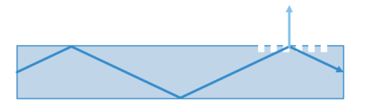
Find the Scattered field subsection. Select the No scattered field check box, as we know that there will not be any scattered wave exiting this boundary.
|
|
1
|
|
3
|
In the Settings window for Matched Boundary Condition, locate the Matched Boundary Condition section.
|
|
4
|
From the Input wave list, choose Second wave, the first wave will be absorbed at this boundary and there will not be any incident wave here.
|
|
1
|
|
3
|
|
4
|
|
5
|
Locate the Impedance Boundary Condition section. From the n list, choose User defined. From the k list, choose User defined. This specifies the refractive index of the air surrounding the waveguide.
|
|
1
|
|
2
|
|
3
|
|
4
|
|
1
|
|
2
|
|
3
|
|
4
|
|
1
|
|
2
|
|
3
|
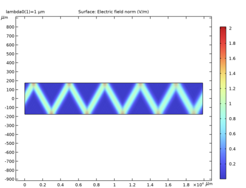
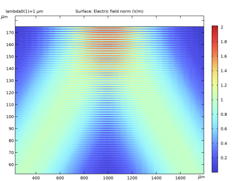
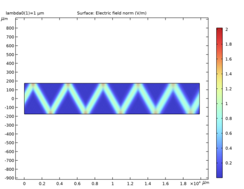
From the Resolution list, choose Extra fine, to resolve the interference patterns close to the top and bottom boundaries.
|
|
4
|
|
1
|
|
2
|
|
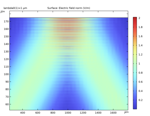
1
|
|
2
|
|
3
|
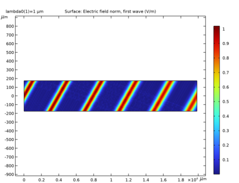
In the Expression text field, type ewbe.normE1, to plot the norm of the electric field for the first wave.
|
|
4
|
|
5
|
|
1
|
|
2
|
|
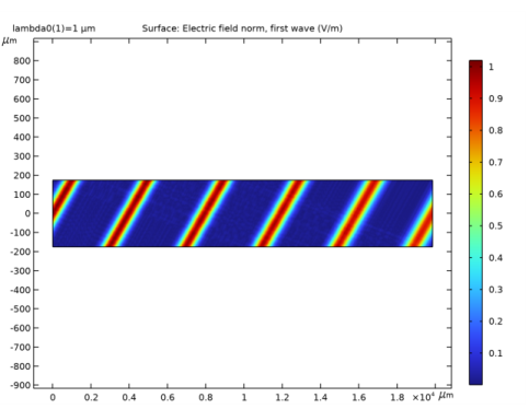
1
|
|
2
|
|
3
|
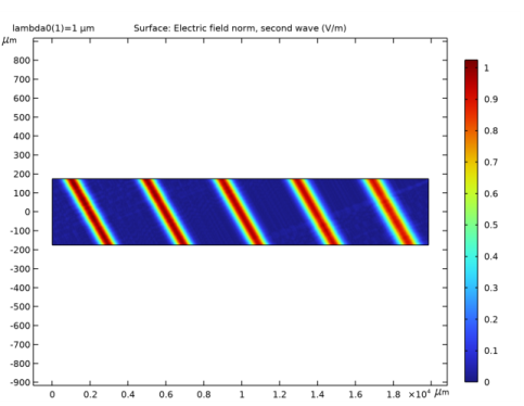
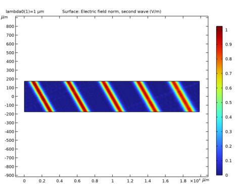
In the Expression text field, type ewbe.normE2, to plot the norm of the electric field for the second wave.
|
|
4
|
|
1
|
|
2
|
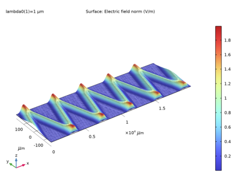
In the Settings window for 2D Plot Group, type Electric Field, Perspective View in the Label text field.
|
|
1
|
In the Model Builder window, expand the Electric Field, Perspective View node, then click Electric Field.
|
|
2
|
|
3
|
|
1
|
|
2
|
|
3
|
|
4
|
|
1
|
|
2
|
|
3
|
|
4
|
|
5
|
|
6
|
Click
|
|
7
|