PDF

Plasmonic Wire Grating
Introduction
A plane electromagnetic wave is incident on a wire grating on a dielectric substrate. The model computes transmission and reflection coefficients for the refraction, specular reflection, and first order diffraction.
Model Definition
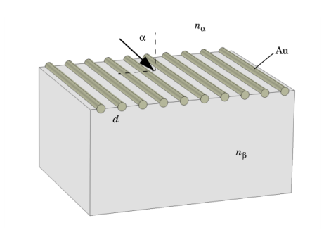
Figure 1 shows the considered grating, with a gold wire on a dielectric material with refractive index nβ. The grating constant, or the distance between the wires, is d. A plane-polarized wave traveling through a medium with refractive index nα is incident on the grating, at an angle α in a plane perpendicular to the grating.
Figure 1: The modeled grating. The model considers a unit cell of a slice through this geometry. The grating is assumed to consist of an infinite number of infinitely long wires.
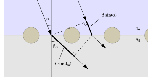
If the wavelengths involved in the model are sufficiently shorter than the grating constant, one or several diffraction orders can be present. The diagram in Figure 2 shows two transmissive paths taken by light incident on adjacent cells of the grating, exactly one grating constant apart.
Figure 2: The geometric path lengths of two transmitted parallel beams. The optical path length is the geometric path length multiplied by the local refractive index.
The criterion for positive interference is that the difference in optical path length along the two paths equals an integer number of vacuum wavelengths, or:
(1)
with m = 0, ±1,± 2,..., λ0 the vacuum wavelength, and βm the transmitted diffracted beam of order m. For m = 0, this reduces to refraction, as described by Snell’s law:
Because the sine functions can only vary between 1 and 1, the existence of higher diffraction order requires that
The model instructions cover only first order diffraction, and are hence only valid under the condition
(2)
Note that for the special cases of perpendicular and grazing incidence, the right-hand side of the inequality evaluates to dnβ and d(nα + nβ), respectively.
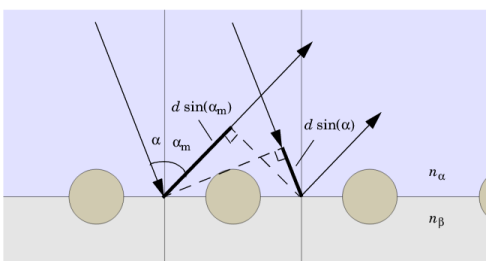
Figure 3 shows the corresponding paths of the reflected light.
Figure 3: The geometric path lengths of two parallel reflected beams.
For positive interference we get
(3)
where αm is the reflected beam of diffraction order m. Setting m = 0 in this equation renders
or specular reflection. The condition for no reflected diffracted beams of order 2 or greater being present is
(4)
The model uses nα = 1 for air and nβ = 1.2 for the dielectric substrate. Allowing for arbitrary angles of incidence and with a grating constant d = 400 nm, Equation 2 sets the validity limit to vacuum wavelengths greater than 440 nm. The model uses λ0 = 441 nm. For the wire, a complex-valued permittivity of 1.75 − 5.4i approximates that of gold at the corresponding frequency.
The performance of the grating depends on the polarization of the incident wave. Therefore both a transverse electric (TE) and a transverse magnetic (TM) case are considered. The TE wave has the electric field component in the z direction, out of the modeling xy-plane. For the TM wave, the electric field vector is pointing in the xy-plane and perpendicular to the direction of propagation, whereas the magnetic field has only a component in the z direction. The angle of incidence is for both cases swept from 0 to π/2, with a pitch of π/40.
Results and Discussion
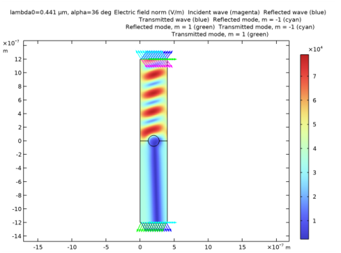
As an example of the output from the model, Figure 4 and Figure 5 show the electric field norm for an angle of incidence equal to π/5, for the TE and TM case respectively.
Figure 4: Electric field norm for TE incidence at π/5.
Figure 5: Electric field norm for TM incidence at π/5.
All the computed transmission and reflection coefficients for TE incidence are plotted in Figure 6. R0, the coefficient for specular reflection, increases rather steadily with the angle of incidence. This is both because of reflection in the material interface and because the wave “sees” the wire as increasingly wider at greater angles — the same effect as achieved by a Venetian blind. T0, the refracted but not diffracted transmission, decreases accordingly. For the considered wavelength to period length ratio, the transmitted diffracted beam T1 is propagating only for nearly perpendicular incidence. The reflected diffraction order R1 would need a shorter wavelength or a larger grating period to show up. Instead, the most prominent diffraction orders are R1 and T1.
The sum of all coefficients is consistently less than 1 due to the dielectric losses in the wire. This is even more apparent for TM incidence, as Figure 7 shows. Here, approximately half of the wave is absorbed in the wire. Another important feature of the TM case is that there is very little specular reflection (R0) around 60 degrees.
Figure 6: Transmission and reflection coefficients for TE incidence.
Figure 7: Transmission and reflection coefficients for TM incidence.
Notes About the COMSOL Implementation
The model is set up for one unit cell of the grating, flanked by Floquet boundary conditions describing the periodicity. As applied, this condition states that the solution on one side of the unit equals the solution on the other side multiplied by a complex-valued phase factor. The phase shift between the boundaries is evaluated from the perpendicular component of the wave vector. Because the periodicity boundaries are parallel with the y-axis, only the x-component is required. Due to the continuity of the field, the phase factor for the refracted and reflected beams is the same as for the incident wave.
Port conditions are used for specifying the incident wave and also for letting the resulting solution leave the model without any nonphysical reflections. In order to achieve perfect transmission through the port boundaries, one port for each mode (m = 0, m = −1, m = 1) in each direction must be present. This gives a total of 6 ports.
The input to each periodic port is an electric or magnetic field amplitude vector and an angle of incidence. The angle of incidence is defined as
where k is the propagation vector of the incident wave, n is the normalized normal vector, k is the wave number, α is the angle of incidence, and z is the unit vector in the z direction. Note that this definition means that the angle of incidence on the opposite sides have opposite signs. To automatically create ports for the diffraction orders, you also provide the refractive index at the port boundary and the maximum frequency (which in this model is the single frequency that is used).
The table below lists the parameters names used in the model. “Internal” means that the variable is not provided as an input parameter.
nα
nβ
α
α1
α-1
β0
β1
β-1
Application Library path: Wave_Optics_Module/Gratings_and_Metamaterials/plasmonic_wire_grating
Modeling Instructions
From the File menu, choose New.
New
In the New window, click  Model Wizard.
Model Wizard
1
In the Model Wizard window, click  2D.
2
In the Select Physics tree, select Optics>Wave Optics>Electromagnetic Waves, Frequency Domain (ewfd).
3
Click Add.
4
Click  Study.
5
In the Select Study tree, select Preset Studies for Selected Physics Interfaces>Wavelength Domain.
6
Global Definitions
Parameters 1
1
In the Model Builder window, under Global Definitions click Parameters 1.
2
In the Settings window for Parameters, locate the Parameters section.
3
Although the angle of incidence will not remain constant at 0, it needs to be specified as a parameter to be accessible to the parametric solver.
Study 1
Step 1: Wavelength Domain
1
In the Model Builder window, under Study 1 click Step 1: Wavelength Domain.
2
In the Settings window for Wavelength Domain, locate the Study Settings section.
3
In the Wavelengths text field, type lam0.
4
Click to expand the Study Extensions section. Select the Auxiliary sweep check box.
5
6
7
Click  Range.
8
In the Range dialog box, type 0[rad] in the Start text field.
9
In the Step text field, type pi/40[rad].
10
In the Stop text field, type (pi/2-pi/40)[rad].
11
Click Replace.
12
In the Settings window for Wavelength Domain, locate the Study Extensions section.
13
Geometry 1
Create the geometry entirely in terms of the grating constant, for easy scalability.
Rectangle 1 (r1)
1
In the Geometry toolbar, click  Rectangle.
2
In the Settings window for Rectangle, locate the Size and Shape section.
3
In the Width text field, type d.
4
In the Height text field, type 3*d.
5
Click  Build Selected.
Rectangle 2 (r2)
1
In the Geometry toolbar, click  Rectangle.
2
In the Settings window for Rectangle, locate the Size and Shape section.
3
In the Width text field, type d.
4
In the Height text field, type 3*d.
5
Locate the Position section. In the y text field, type -3*d.
6
Click  Build Selected.
Circle 1 (c1)
1
In the Geometry toolbar, click  Circle.
2
In the Settings window for Circle, locate the Size and Shape section.
3
In the Radius text field, type d/5.
4
Locate the Position section. In the x text field, type d/2.
5
Click  Build Selected.
6
Click the  Zoom Extents button in the Graphics toolbar.
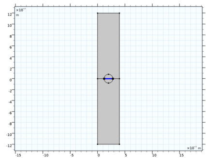
The geometry now consists of two rectangular domains for the air and the dielectric, and a circle centered on their intersection. You can remove the line through the circle if you first create a union of the objects.
Union 1 (uni1)
1
In the Geometry toolbar, click  Booleans and Partitions and choose Union.
2
Click in the Graphics window and then press Ctrl+A to select all objects.
3
In the Settings window for Union, click  Build Selected.
Delete Entities 1 (del1)
1
In the Model Builder window, right-click Geometry 1 and choose Delete Entities.
2
On the object uni1, select Boundary 6 only. This is the horizontal diameter of the circle in the center of the geometry.
3
In the Settings window for Delete Entities, click  Build Selected.
Form Union (fin)
1
In the Model Builder window, click Form Union (fin).
2
In the Settings window for Form Union/Assembly, click  Build Selected.
Materials
Air
1
In the Model Builder window, under Component 1 (comp1) right-click Materials and choose Blank Material.
2
In the Settings window for Material, type Air in the Label text field.
3
Locate the Material Contents section. In the table, enter the following settings:
Dielectric
1
Right-click Materials and choose Blank Material.
2
In the Settings window for Material, type Dielectric in the Label text field.
3
4
Locate the Material Contents section. In the table, enter the following settings:
Add Material
1
In the Home toolbar, click  Add Material to open the Add Material window.
2
Go to the Add Material window.
3
In the tree, select Optical>Inorganic Materials>Au - Gold>Models and simulations>Au (Gold) (Rakic et al. 1998: Brendel-Bormann model; n,k 0.248-6.20 um), to select gold from the Optical Materials Database.
4
Click Add to Component in the window toolbar.
5
In the Home toolbar, click  Add Material to close the Add Material window.
Materials
Au (Gold) (Rakic et al. 1998: Brendel-Bormann model; n,k 0.248-6.20 um) (mat3)
Select Domain 3 only.
Electromagnetic Waves, Frequency Domain (ewfd)
In the first version of this model, you will assume a TE-polarized wave. This means that Ex and Ey will be zero throughout the geometry, and that you consequently only need to solve for Ez.
1
In the Model Builder window, under Component 1 (comp1) click Electromagnetic Waves, Frequency Domain (ewfd).
2
In the Settings window for Electromagnetic Waves, Frequency Domain, locate the Components section.
3
From the Electric field components solved for list, choose Out-of-plane vector.
Port 1
Now define the excitation port. A periodic port assumes that the structure is periodic and simplifies the setup of ports for the diffraction orders.
1
In the Physics toolbar, click  Boundaries and choose Port.
2
It might be easier to select the correct boundary by using the Selection List window. To open this window, in the Home toolbar click Windows and choose Selection List. (If you are running the cross-platform desktop, you find Windows in the main menu.)
3
In the Settings window for Port, locate the Port Properties section.
4
From the Type of port list, choose Periodic.
For the first port, wave excitation is on by default.
Notice that you define the electric field by only setting the amplitude. A phase factor should not be entered.
5
Locate the Port Mode Settings section. Specify the E0 vector as
6
In the α text field, type alpha.
7
Locate the Automatic Diffraction Order Calculation section. In the n text field, type na.
The order in which you set up the ports will determine how the S-parameters are labeled. You have just created Port 1 for the excitation. If you set up the next port for the transmission of the purely refracted beam, the S21-parameter will contain information on the zero order transmission.
Notice that for the exciting port (Port 1) there are no propagating diffraction orders for normal incidence. Instead, manually add the Diffraction Order port subfeatures.
8
Clear the Include in automatic diffraction order calculation check box, to not remove the manually added Diffraction Order port subfeatures below this port when you later will click the Add Diffraction Orders button.
Port 2
1
In the Physics toolbar, click  Boundaries and choose Port.
2
3
In the Settings window for Port, locate the Port Properties section.
4
From the Type of port list, choose Periodic.
5
Locate the Port Mode Settings section. Specify the E0 vector as
For the listener port you only need to provide the refractive index for the automatic generation of Diffration Order ports. The propagation angle is automatically determined from Snell’s law, give the angle of incidence for the exciting periodic port and the refractive indices provided for the exciting port and this listener port.
6
Locate the Automatic Diffraction Order Calculation section. In the n text field, type nb.
Port 1
Now manually add the ports for the reflected diffraction orders.
1
In the Model Builder window, click Port 1.
Diffraction Order 1
1
In the Physics toolbar, click  Attributes and choose Diffraction Order.
2
In the Settings window for Diffraction Order, locate the Port Mode Settings section.
3
From the Components list, choose Out-of-plane vector.
4
In the m text field, type -1.
Diffraction Order 2
1
Right-click Diffraction Order 1 and choose Duplicate.
2
In the Settings window for Diffraction Order, locate the Port Mode Settings section.
3
In the m text field, type 1.
Port 1
Finally, automatically add the ports for the transmitted diffraction orders.
1
In the Model Builder window, click Port 1.
2
In the Settings window for Port, locate the Automatic Diffraction Order Calculation section.
3
Click Add Diffraction Orders.
Inspect the Diffraction Order port subfeatures by expanding the Port 2 node.
Periodic Condition 1
1
In the Model Builder window, expand the Port 2 node.
2
Right-click Electromagnetic Waves, Frequency Domain (ewfd) and choose Periodic Condition.
3
4
In the Settings window for Periodic Condition, locate the Periodicity Settings section.
5
From the Type of periodicity list, choose Floquet periodicity.
The wave vector in the direction for the periodicity is used by the periodic port. Thus, you can use that wave vector also for the Floquet periodic condition.
6
From the k-vector for Floquet periodicity list, choose From periodic port.
Study 1
To set up the study to sweep for the angle of incidence, some modifications of the solver are required.
In the Home toolbar, click  Compute.
Results
Add arrow plots for the incident wave vector of the excitation port and the mode wave vector of each diffraction order.
Arrow Line 1
1
Right-click Electric Field (ewfd) and choose Arrow Line.
2
In the Settings window for Arrow Line, click Replace Expression in the upper-right corner of the Expression section. From the menu, choose Component 1 (comp1)>Electromagnetic Waves, Frequency Domain>Ports>ewfd.kIncx_1,ewfd.kIncy_1 - Incident wave vector.
3
Locate the Coloring and Style section. From the Color list, choose Magenta.
4
Locate the Expression section. Select the Description check box.
5
In the associated text field, type Incident wave (magenta).
Arrow Line 2
1
Right-click Electric Field (ewfd) and choose Arrow Line.
2
In the Settings window for Arrow Line, click Replace Expression in the upper-right corner of the Expression section. From the menu, choose Component 1 (comp1)>Electromagnetic Waves, Frequency Domain>Ports>ewfd.kModex_1,ewfd.kModey_1 - Port mode wave vector.
3
Locate the Coloring and Style section. From the Color list, choose Blue.
4
Locate the Expression section. Select the Description check box.
5
Arrow Line 3
1
Right-click Electric Field (ewfd) and choose Arrow Line.
2
In the Settings window for Arrow Line, click Replace Expression in the upper-right corner of the Expression section. From the menu, choose Component 1 (comp1)>Electromagnetic Waves, Frequency Domain>Ports>ewfd.kModex_2,ewfd.kModey_2 - Port mode wave vector.
3
Locate the Coloring and Style section. From the Color list, choose Blue.
4
Locate the Expression section. Select the Description check box.
5
In the associated text field, type Transmitted wave (blue).
Arrow Line 4
1
Right-click Electric Field (ewfd) and choose Arrow Line.
2
In the Settings window for Arrow Line, click Replace Expression in the upper-right corner of the Expression section. From the menu, choose Component 1 (comp1)>Electromagnetic Waves, Frequency Domain>Ports>ewfd.kModex_3,ewfd.kModey_3 - Port mode wave vector.
3
Locate the Coloring and Style section. From the Color list, choose Cyan.
4
Locate the Expression section. Select the Description check box.
5
In the associated text field, type Reflected mode, m = -1 (cyan).
Arrow Line 5
1
Right-click Arrow Line 4 and choose Duplicate.
2
In the Settings window for Arrow Line, click Replace Expression in the upper-right corner of the Expression section. From the menu, choose Component 1 (comp1)>Electromagnetic Waves, Frequency Domain>Ports>ewfd.kModex_4,ewfd.kModey_4 - Port mode wave vector.
3
Locate the Coloring and Style section. From the Color list, choose Green.
4
Locate the Expression section. In the Description text field, type Reflected mode, m = 1 (green).
Arrow Line 6
1
In the Model Builder window, under Results>Electric Field (ewfd) right-click Arrow Line 4 and choose Duplicate.
2
In the Settings window for Arrow Line, locate the Expression section.
3
In the X component text field, type ewfd.kModex_5.
4
In the Y component text field, type ewfd.kModey_5.
5
In the Description text field, type Transmitted mode, m = -1 (cyan).
Arrow Line 7
1
In the Model Builder window, under Results>Electric Field (ewfd) right-click Arrow Line 5 and choose Duplicate.
2
In the Settings window for Arrow Line, locate the Expression section.
3
In the X component text field, type ewfd.kModex_6.
4
In the Y component text field, type ewfd.kModey_6.
5
In the Description text field, type Transmitted mode, m = 1 (green).
TE Electric Field
1
In the Model Builder window, under Results click Electric Field (ewfd).
2
In the Settings window for 2D Plot Group, type TE Electric Field in the Label text field.
The default plot shows the electric field norm for the last solution, almost tangential incidence. Look at a more interesting angle of incidence.
3
Locate the Data section. From the Parameter value (alpha (deg)) list, choose 36.
Make the title slightly shorter.
4
Click to expand the Title section. From the Title type list, choose Custom.
5
Find the Type and data subsection. Clear the Type check box.
6
In the TE Electric Field toolbar, click  Plot.
7
Click the  Zoom Extents button in the Graphics toolbar. The plot should now look like Figure 4.
TE Reflectance, Transmittance, and Absorptance
Modify the generated 1D plot of the diffraction efficiencies for the different orders versus the angle of incidence.
1
In the Model Builder window, under Results click Reflectance, Transmittance, and Absorptance (ewfd).
2
In the Settings window for 1D Plot Group, type TE Reflectance, Transmittance, and Absorptance in the Label text field.
3
Click to expand the Title section. From the Title type list, choose Manual.
4
In the Title text area, type Reflectance and Transmittance of TE Wave.
Global 1
1
In the Model Builder window, expand the TE Reflectance, Transmittance, and Absorptance node, then click Global 1.
2
In the Settings window for Global, click to expand the Coloring and Style section.
3
Find the Line markers subsection. From the Marker list, choose Cycle.
Since it is possible to use subscript notation in the legends and the polarization is known, the legends can be shortened.
4
Click to expand the Legends section. From the Legends list, choose Manual.
5
6
In the TE Reflectance, Transmittance, and Absorptance toolbar, click  Plot. The plot should now look like Figure 6.
Electromagnetic Waves, Frequency Domain (ewfd)
The remaining instructions show how to alter the physics so that you solve for an incident TM wave.
1
In the Model Builder window, under Component 1 (comp1) click Electromagnetic Waves, Frequency Domain (ewfd).
2
In the Settings window for Electromagnetic Waves, Frequency Domain, locate the Components section.
3
From the Electric field components solved for list, choose In-plane vector.
You will now solve for Ex and Ey instead of Ez; for a TM wave, Ez is zero.
Port 1
The easiest way to specify a TM wave is to define the magnetic field, since only the z component is used.
1
In the Model Builder window, under Component 1 (comp1)>Electromagnetic Waves, Frequency Domain (ewfd) click Port 1.
2
In the Settings window for Port, locate the Port Mode Settings section.
3
From the Input quantity list, choose Magnetic field.
4
Specify the H0 vector as
5
Locate the Automatic Diffraction Order Calculation section. Click Add Diffraction Orders, to update the Diffraction Order port subfeatures below Port 2.
Diffraction Order 1
The Diffraction Order port subfeatures below this port (Port 1) must be updated manually.
1
In the Model Builder window, click Diffraction Order 1.
2
In the Settings window for Diffraction Order, locate the Port Mode Settings section.
3
From the Components list, choose In-plane vector.
Diffraction Order 2
1
In the Model Builder window, click Diffraction Order 2.
2
In the Settings window for Diffraction Order, locate the Port Mode Settings section.
3
From the Components list, choose In-plane vector.
Port 2
1
In the Model Builder window, under Component 1 (comp1)>Electromagnetic Waves, Frequency Domain (ewfd) click Port 2.
2
In the Settings window for Port, locate the Port Mode Settings section.
3
From the Input quantity list, choose Magnetic field.
4
Specify the H0 vector as
Root
Add a new study in order not to overwrite the TE solution.
Add Study
1
In the Home toolbar, click  Add Study to open the Add Study window.
2
Go to the Add Study window.
3
Find the Studies subsection. In the Select Study tree, select Preset Studies for Selected Physics Interfaces>Wavelength Domain.
4
Click Add Study in the window toolbar.
5
In the Home toolbar, click  Add Study to close the Add Study window.
Study 2
Step 1: Wavelength Domain
1
In the Settings window for Wavelength Domain, locate the Study Settings section.
2
In the Wavelengths text field, type lam0.
3
Locate the Study Extensions section. Select the Auxiliary sweep check box.
4
5
6
Click  Range.
7
In the Range dialog box, type 0[rad] in the Start text field.
8
In the Step text field, type pi/40[rad].
9
In the Stop text field, type (pi/2-pi/40)[rad].
10
Click Replace.
11
In the Settings window for Wavelength Domain, locate the Study Extensions section.
12
13
In the Home toolbar, click  Compute.
Results
Arrow Line 1
1
Right-click Electric Field (ewfd) and choose Arrow Line.
2
In the Settings window for Arrow Line, click Replace Expression in the upper-right corner of the Expression section. From the menu, choose Component 1 (comp1)>Electromagnetic Waves, Frequency Domain>Ports>ewfd.kIncx_1,ewfd.kIncy_1 - Incident wave vector.
3
Locate the Coloring and Style section. From the Color list, choose Magenta.
4
Locate the Expression section. Select the Description check box.
5
In the associated text field, type Incident wave (magenta).
Arrow Line 2
1
Right-click Electric Field (ewfd) and choose Arrow Line.
2
In the Settings window for Arrow Line, click Replace Expression in the upper-right corner of the Expression section. From the menu, choose Component 1 (comp1)>Electromagnetic Waves, Frequency Domain>Ports>ewfd.kModex_1,ewfd.kModey_1 - Port mode wave vector.
3
Locate the Coloring and Style section. From the Color list, choose Blue.
4
Locate the Expression section. Select the Description check box.
5
Arrow Line 3
1
Right-click Electric Field (ewfd) and choose Arrow Line.
2
In the Settings window for Arrow Line, click Replace Expression in the upper-right corner of the Expression section. From the menu, choose Component 1 (comp1)>Electromagnetic Waves, Frequency Domain>Ports>ewfd.kModex_2,ewfd.kModey_2 - Port mode wave vector.
3
Locate the Coloring and Style section. From the Color list, choose Blue.
4
Locate the Expression section. Select the Description check box.
5
In the associated text field, type Transmitted wave (blue).
Arrow Line 4
1
Right-click Electric Field (ewfd) and choose Arrow Line.
2
In the Settings window for Arrow Line, click Replace Expression in the upper-right corner of the Expression section. From the menu, choose Component 1 (comp1)>Electromagnetic Waves, Frequency Domain>Ports>ewfd.kModex_3,ewfd.kModey_3 - Port mode wave vector.
3
Locate the Coloring and Style section. From the Color list, choose Cyan.
4
Locate the Expression section. Select the Description check box.
5
In the associated text field, type Reflected mode, m = -1 (cyan).
Arrow Line 5
1
Right-click Arrow Line 4 and choose Duplicate.
2
In the Settings window for Arrow Line, click Replace Expression in the upper-right corner of the Expression section. From the menu, choose Component 1 (comp1)>Electromagnetic Waves, Frequency Domain>Ports>ewfd.kModex_4,ewfd.kModey_4 - Port mode wave vector.
3
Locate the Coloring and Style section. From the Color list, choose Green.
4
Locate the Expression section. In the Description text field, type Reflected mode, m = 1 (green).
Arrow Line 6
1
In the Model Builder window, under Results>Electric Field (ewfd) right-click Arrow Line 4 and choose Duplicate.
2
In the Settings window for Arrow Line, locate the Expression section.
3
In the X component text field, type ewfd.kModex_5.
4
In the Y component text field, type ewfd.kModey_5.
5
In the Description text field, type Transmitted mode, m = -1 (cyan).
Arrow Line 7
1
In the Model Builder window, under Results>Electric Field (ewfd) right-click Arrow Line 5 and choose Duplicate.
2
In the Settings window for Arrow Line, locate the Expression section.
3
In the X component text field, type ewfd.kModex_6.
4
In the Y component text field, type ewfd.kModey_6.
5
In the Description text field, type Transmitted mode, m = 1 (green).
TM Electric Field
1
In the Model Builder window, under Results click Electric Field (ewfd).
2
In the Settings window for 2D Plot Group, type TM Electric Field in the Label text field.
3
Locate the Data section. From the Parameter value (alpha (deg)) list, choose 36.
4
Locate the Title section. From the Title type list, choose Custom.
5
Find the Type and data subsection. Clear the Type check box.
6
In the TM Electric Field toolbar, click  Plot.
7
Click the  Zoom Extents button in the Graphics toolbar. You have now reproduced Figure 5.
TM Reflectance, Transmittance, and Absorptance
1
In the Model Builder window, under Results click Reflectance, Transmittance, and Absorptance (ewfd).
2
In the Settings window for 1D Plot Group, type TM Reflectance, Transmittance, and Absorptance in the Label text field.
3
Locate the Title section. From the Title type list, choose Manual.
4
In the Title text area, type Reflectance and Transmittance of TM Wave.
Global 1
1
In the Model Builder window, expand the TM Reflectance, Transmittance, and Absorptance node, then click Global 1.
2
In the Settings window for Global, locate the Coloring and Style section.
3
Find the Line markers subsection. From the Marker list, choose Cycle.
Also for this plot, shorten the legends.
4
Locate the Legends section. From the Legends list, choose Manual.
5
6
In the TM Reflectance, Transmittance, and Absorptance toolbar, click  Plot. Compare the resulting plot with that in Figure 7.