|
|
|
|
1
|
|
2
|
|
3
|
Click Add.
|
|
4
|
Click
|
|
5
|
In the Select Study tree, select Preset Studies for Selected Physics Interfaces>Semiconductor Equilibrium.
|
|
6
|
Click
|
|
1
|
|
2
|
|
3
|
|
1
|
|
2
|
|
1.6E-8 Ω·m²
|
|||
|
4.7E-10 Ω·m²
|
|||
|
4
|
|
1
|
|
2
|
|
1
|
|
2
|
In the Settings window for Rectangle, type Rectangle 1 - Device outline (half cell) in the Label text field.
|
|
3
|
|
4
|
|
5
|
|
6
|
Click to expand the Layers section. In the table, enter the following settings:
|
|
1
|
|
2
|
|
3
|
|
4
|
|
5
|
|
6
|
|
1
|
|
2
|
|
3
|
|
4
|
|
5
|
|
1
|
|
2
|
In the Settings window for Difference, type Difference 1 - Device outline minus trench in the Label text field.
|
|
3
|
Select the object r1 only.
|
|
4
|
Locate the Difference section. Find the Objects to subtract subsection. Click to select the
|
|
5
|
|
1
|
|
2
|
In the Settings window for Point, type Point 1 - Emitter contact & doping boundary in the Label text field.
|
|
3
|
|
4
|
|
1
|
|
2
|
|
3
|
|
4
|
|
5
|
|
1
|
|
2
|
|
3
|
|
4
|
|
5
|
|
6
|
|
1
|
|
2
|
|
3
|
|
1
|
In the Model Builder window, under Component 1 (comp1)>Geometry 1 right-click Circle 1 - Trench (c1) and choose Duplicate.
|
|
2
|
|
3
|
|
4
|
|
5
|
|
6
|
|
1
|
|
2
|
On the object c2, select Boundaries 3 and 4 only.
|
|
1
|
|
2
|
In the Settings window for Line Segment, type Line Segment 1 - Mesh help line in the Label text field.
|
|
3
|
|
4
|
|
5
|
|
6
|
|
7
|
|
1
|
|
2
|
On the object fin, select Boundaries 8, 10, 15–18, 23, 25, 31, and 33 only.
|
|
3
|
|
1
|
|
2
|
|
3
|
|
4
|
|
5
|
|
1
|
|
2
|
|
3
|
|
4
|
|
1
|
|
2
|
|
3
|
|
4
|
|
1
|
|
2
|
|
3
|
|
4
|
Locate the Material Properties section. From the Eg,0 list, choose User defined. In the associated text field, type Eg0.
|
|
5
|
|
6
|
|
7
|
Locate the Mobility Model section. From the μn list, choose Electron mobility, Caughey-Thomas (semi/smm1/mmct1).
|
|
8
|
|
9
|
|
10
|
|
1
|
|
2
|
In the Settings window for Analytic Doping Model, type Analytic Doping Model - n-base in the Label text field.
|
|
4
|
|
5
|
|
1
|
|
2
|
In the Settings window for Analytic Doping Model, type Analytic Doping Model - n-buffer in the Label text field.
|
|
4
|
|
5
|
|
1
|
|
2
|
In the Settings window for Analytic Doping Model, type Analytic Doping Model - p+ collector in the Label text field.
|
|
4
|
|
1
|
|
2
|
In the Settings window for Geometric Doping Model, type Geometric Doping Model - p-base in the Label text field.
|
|
4
|
|
5
|
|
6
|
|
1
|
In the Model Builder window, expand the Geometric Doping Model - p-base node, then click Boundary Selection for Doping Profile 1.
|
|
1
|
|
2
|
In the Settings window for Geometric Doping Model, type Geometric Doping Model - p+ emitter in the Label text field.
|
|
4
|
|
5
|
|
6
|
|
1
|
In the Model Builder window, expand the Geometric Doping Model - p+ emitter node, then click Boundary Selection for Doping Profile 1.
|
|
1
|
|
2
|
In the Settings window for Geometric Doping Model, type Geometric Doping Model - n+ emitter in the Label text field.
|
|
4
|
|
5
|
|
6
|
|
7
|
|
1
|
In the Model Builder window, expand the Geometric Doping Model - n+ emitter node, then click Boundary Selection for Doping Profile 1.
|
|
1
|
|
2
|
|
3
|
|
4
|
Locate the Shockley-Read-Hall Recombination section. From the τn list, choose User defined. In the associated text field, type tau0.
|
|
5
|
|
1
|
|
2
|
|
4
|
|
5
|
|
6
|
|
1
|
|
2
|
|
4
|
|
5
|
|
6
|
|
7
|
|
1
|
|
3
|
|
4
|
|
5
|
|
6
|
|
7
|
|
1
|
|
2
|
|
4
|
Click to expand the Control Entities section. Clear the Smooth across removed control entities check box.
|
|
1
|
|
2
|
|
3
|
|
4
|
|
5
|
|
6
|
|
1
|
|
2
|
|
3
|
Click the Custom button.
|
|
4
|
|
5
|
|
6
|
|
7
|
|
8
|
|
1
|
|
2
|
|
4
|
|
1
|
|
2
|
|
3
|
|
4
|
|
5
|
|
6
|
|
1
|
|
2
|
|
4
|
|
1
|
|
2
|
|
3
|
|
4
|
|
5
|
|
1
|
|
3
|
|
4
|
|
6
|
Click to expand the Control Entities section. Clear the Smooth across removed control entities check box.
|
|
1
|
|
2
|
|
3
|
|
5
|
Click to expand the Control Entities section. Clear the Smooth across removed control entities check box.
|
|
6
|
|
1
|
|
3
|
|
4
|
|
5
|
|
6
|
|
7
|
|
8
|
|
1
|
|
2
|
|
3
|
|
5
|
|
6
|
|
1
|
|
2
|
|
4
|
|
5
|
|
6
|
|
1
|
|
2
|
|
4
|
|
5
|
|
1
|
|
2
|
In the Settings window for Distribution, type Distribution 3 - Left surface in the Label text field.
|
|
4
|
|
5
|
|
6
|
|
7
|
|
1
|
|
2
|
In the Settings window for Distribution, type Distribution 4 - Right surface in the Label text field.
|
|
4
|
|
5
|
|
6
|
|
1
|
|
2
|
In the Settings window for Distribution, type Distribution 5 - Bottom surface in the Label text field.
|
|
4
|
|
5
|
|
6
|
|
7
|
|
1
|
|
2
|
|
3
|
|
5
|
Click to expand the Control Entities section. Clear the Smooth across removed control entities check box.
|
|
6
|
|
7
|
|
1
|
|
3
|
|
4
|
|
6
|
|
1
|
|
2
|
|
3
|
|
4
|
|
1
|
|
2
|
|
4
|
|
5
|
|
6
|
|
7
|
|
1
|
|
2
|
|
4
|
|
5
|
|
1
|
|
2
|
In the Settings window for Distribution, type Distribution 3 - p+ collector in the Label text field.
|
|
4
|
|
5
|
|
6
|
|
7
|
|
8
|
|
1
|
|
2
|
|
3
|
|
4
|
Click
|
|
6
|
|
1
|
In the Model Builder window, expand the Study 1>Solver Configurations>Solution 1 (sol1) node, then click Dependent Variables 2.
|
|
2
|
|
3
|
|
4
|
In the Model Builder window, expand the Study 1>Solver Configurations>Solution 1 (sol1)>Dependent Variables 2 node, then click Voltage drop across contact (comp1.semi.V_dae).
|
|
5
|
|
6
|
|
7
|
|
1
|
|
2
|
|
3
|
|
4
|
|
5
|
|
6
|
|
7
|
|
8
|
|
9
|
|
1
|
|
2
|
|
3
|
|
4
|
|
1
|
|
2
|
|
3
|
|
4
|
|
5
|
|
6
|
|
7
|
|
1
|
|
2
|
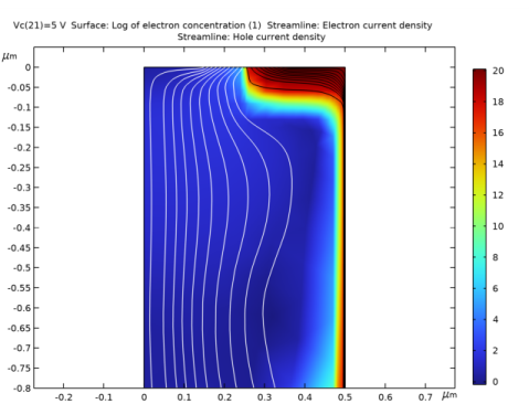
In the Settings window for 2D Plot Group, type Electron Concentration & Current Streamlines in the Label text field.
|
|
3
|
|
1
|
|
2
|
|
3
|
|
4
|
|
5
|
|
6
|
|
7
|
Click
|
|
1
|
In the Model Builder window, right-click Electron Concentration & Current Streamlines and choose Streamline.
|
|
2
|
In the Settings window for Streamline, type Streamline 1 - Electron current in the Label text field.
|
|
3
|
Click Replace Expression in the upper-right corner of the Expression section. From the menu, choose Component 1 (comp1)>Semiconductor>Currents and charge>Electron current>semi.JnX,semi.JnY - Electron current density.
|
|
4
|
|
1
|
|
2
|
|
3
|
Click Replace Expression in the upper-right corner of the Expression section. From the menu, choose Component 1 (comp1)>Semiconductor>Currents and charge>Hole current>semi.JpX,semi.JpY - Hole current density.
|
|
4
|
|
6
|
Locate the Coloring and Style section. Find the Point style subsection. From the Color list, choose White.
|
|
7
|