
|
|
|
|
|
If the entire time history is of interest, then the time-dependent study should use a physical solution as the initial condition. Usually, this is done by adding a Stationary study step before the time dependent study step. In addition, it is sometimes necessary to turn off the Consistent initialization under the Time Stepping section of the settings window for the Time-Dependent Solver node under the Solver Configurations tree structure.
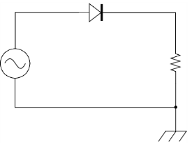
Forward Recovery of a PIN Diode (Application Library path Semiconductor_Module/Device_Building_Blocks/pin_forward_recovery)
Reverse Recovery of a PIN Diode (Application Library path Semiconductor_Module/Device_Building_Blocks/pin_reverse_recovery)
|
|
1
|
|
2
|
|
3
|
Click Add.
|
|
4
|
|
5
|
Click Add.
|
|
6
|
Click
|
|
7
|
|
8
|
Click
|
|
1
|
|
2
|
|
3
|
|
4
|
Browse to the model’s Application Libraries folder and double-click the file pn_diode_circuit_parameters.txt.
|
|
1
|
|
2
|
|
3
|
|
1
|
|
2
|
|
3
|
|
4
|
|
5
|
|
1
|
|
2
|
|
3
|
|
4
|
|
5
|
|
1
|
|
2
|
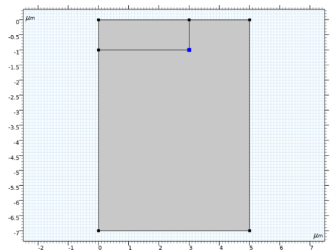
On the object r2, select Point 2 only.
|
|
3
|
|
4
|
|
1
|
|
2
|
|
3
|
|
4
|
|
1
|
|
2
|
|
3
|
|
4
|
|
5
|
|
1
|
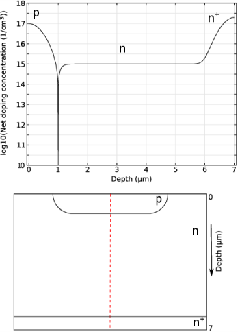
In the Model Builder window, under Component 1 (comp1) right-click Semiconductor (semi) and choose Doping>Analytic Doping Model.
|
|
2
|
|
3
|
|
4
|
|
5
|
|
1
|
|
2
|
|
3
|
|
4
|
|
5
|
|
6
|
|
7
|
|
8
|
|
9
|
|
1
|
|
2
|
|
3
|
|
4
|
|
5
|
|
6
|
|
7
|
|
8
|
|
1
|
|
2
|
|
3
|
|
1
|
|
3
|
|
4
|
|
1
|
|
1
|
|
2
|
|
4
|
|
1
|
|
2
|
|
4
|
|
5
|
|
6
|
|
1
|
|
2
|
|
4
|
|
1
|
|
2
|
|
3
|
Click
|
|
4
|
|
5
|
|
6
|
Click Replace.
|
|
1
|
|
2
|
|
3
|
|
4
|
|
5
|
|
6
|
|
1
|
|
2
|
|
3
|
|
4
|
|
5
|
|
1
|
|
2
|
|
3
|
|
4
|
|
5
|
|
6
|
|
1
|
|
2
|
|
3
|
|
4
|
|
5
|
|
1
|
|
2
|
|
3
|
|
4
|
|
1
|
|
2
|
|
3
|
|
4
|
|
5
|
|
1
|
|
2
|
Click
|
|
3
|
|
4
|
|
5
|
Click Replace.
|
|
6
|
|
7
|
|
8
|
|
9
|
Locate the Physics and Variables Selection section. In the table, clear the Solve for check boxes for Semiconductor (semi) and Electrical Circuit (cir).
|
|
10
|
|
1
|
|
2
|
|
3
|
|
4
|
Click OK.
|
|
5
|
|
6
|
|
7
|
|
8
|
|
9
|
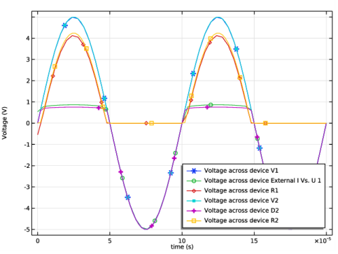
In the associated text field, type time (s).
|
|
10
|
|
11
|
In the associated text field, type Voltage (V).
|
|
12
|
|
1
|
|
2
|
|
3
|
|
4
|
Click Replace Expression in the upper-right corner of the y-Axis Data section. From the menu, choose Component 1 (comp1)>Electrical Circuit>Devices>V1>cir.V1_v - Voltage across device V1 - V.
|
|
5
|
|
6
|
Click to expand the Coloring and Style section. Find the Line markers subsection. From the Marker list, choose Cycle.
|
|
1
|
|
2
|
|
3
|
|
4
|
|
5
|
Locate the Coloring and Style section. Find the Line markers subsection. From the Marker list, choose Cycle.
|
|
6
|