PDF

3D Density-Gradient Simulation of a Nanowire MOSFET
This 3D model of a nanowire MOSFET employs the density-gradient theory to add the effect of quantum confinement to the conventional drift-diffusion formulation, without requiring excessively high computational costs. The oxide layer is simulated explicitly with geometric domains, and quantum confinement at the silicon-oxide interface is accounted for via a dedicated boundary condition. The density-gradient effective mass is anisotropic. Various selection utilities are used to simplify the assignment of physics settings and plot selections. The result matches well with the Id-Vg curves and electron density profiles published in the reference paper.
Introduction
As the semiconductor fabrication technology progresses to produce smaller and smaller devices, the effect of quantum confinement becomes more and more important. This tutorial follows the approach described in Ref. 1 to compute the electron density distribution and drain current as a function of the gate voltage of a Si nanowire MOSFET using the density-gradient theory (as reviewed in Ref. 2).
Model Definition
The model computes the DC characteristics and the electron density profile along the transverse and longitudinal centerlines of a Si nanowire MOSFET, to be compared with Fig. 2, 4, and 5 in Ref. 1. The effects of changing the value of the longitudinal effective mass are shown in those figures.
Not all simulation details are given in the paper. Nevertheless, the approach described in the paper is followed as closely as possible. In particular, the treatment of the potential barrier at the silicon-oxide interface follows the one discussed in Ref. 3. When a parameter is not listed, a typical value found in the literature is used in the model. The silicon material data built in the Semiconductor Module are used, with constant mobility. The gate metal work function and the drain voltage are selected to best match the Id-Vg curves in the reference paper. The section Modeling Instructions lists all the parameters used in the model.
The channel of the simulated structure is formed by a Si nanowire with a 3.2 nm square cross section, surrounded by an oxide layer of thickness 0.8 nm. The length of the channel is 4 nm. (See Fig. 1 in Ref. 1.) The source and drain lengths are arbitrarily set at 15 nm, long enough to provide the comparison with the figures in the reference paper.
The oxide layer is modeled explicitly as domains using the Charge Conservation domain condition. The quantum confinement effect for the silicon-oxide interface is added by selecting the Potential barrier option for the Insulator Interface boundary condition, based on Ref. 3. The temperature is assumed to be 300 K. Maxwell-Boltzmann statistics is used, as indicated by Eq. (2) in Ref. 1.
The density-gradient effective mass is anisotropic in this model. This is done by selecting the Diagonal option under the section Material Properties, Density-Gradient in the settings window for the Semiconductor Material Model domain condition.
For the ease of meshing and plotting along the centerlines, some extra layers are created in the 3D geometry. Various Selection functionalities under both the Geometry and the Definitions nodes are then used to group the multiple geometric entities into different regions for convenient assignment of domain conditions, boundary conditions, and plot selections.
To reduce the computation time and file size, a relatively coarse mesh is used in this tutorial. Interested users are encouraged to perform mesh refinement studies by parameterizing the settings of the Distribution nodes used in the meshing sequence.
See the comments in the section Modeling Instructions for more detailed discussions on the model construction, meshing techniques, solution processes, and result visualization.
Results and Discussion
Figure 1 shows the drain current as a function of the gate voltage for a set of longitudinal effective mass values, to be compared with Fig. 2 in Ref. 1. The general trend and subthreshold slopes compare well, with some minor differences in the magnitude of the current.
Figure 1: Drain current versus gate voltage curves for a few effective mass values.
Figure 2 and Figure 3 plot the electron concentration profiles along the longitudinal and transverse centerlines, which compares well with Fig. 4 and 5 in the reference paper.
Figure 2: Electron concentration profile along the longitudinal centerline.
Figure 3: Electron concentration profile along the transverse centerline.
References
1. A.R. Brown, A. Martinez, N. Seoane, and A. Asenov, “Comparison of Density Gradient and NEGF for 3D Simulation of a Nanowire MOSFET,” Proc. 2009 Spanish Conf. Elec. Dev., p. 140, Feb. 11–13, 2009.
2. M.G. Ancona, “Density-gradient theory: a macroscopic approach to quantum confinement and tunneling in semiconductor devices,” J. Comput. Electron., vol. 10, p. 65, 2011.
3. S. Jin, Y.J. Park, and H.S. Min, “Simulation of Quantum Effects in the Nano-scale Semiconductor Device,” J. Semicond. Tech. Sci., vol. 4, no. 1, p. 32, 2004.
Application Library path: Semiconductor_Module/Transistors/nanowire_density_gradient_3d
Modeling Instructions
From the File menu, choose New.
New
In the New window, click  Model Wizard.
Model Wizard
1
In the Model Wizard window, click  3D.
2
In the Select Physics tree, select Semiconductor>Semiconductor (semi).
3
Click Add.
4
Click  Study.
The Semiconductor Equilibrium study step is suitable either to solve for systems known to be in thermal equilibrium, or, in this case, to provide a good initial condition for subsequent gate voltage sweeps.
5
In the Select Study tree, select Preset Studies for Selected Physics Interfaces>Semiconductor Equilibrium.
6
Geometry 1
The Model Wizard starts the COMSOL Desktop at the Geometry node. Use this chance to select a convenient length unit. Then enter some dimensional parameters for building the geometry.
1
In the Model Builder window, under Component 1 (comp1) click Geometry 1.
2
In the Settings window for Geometry, locate the Units section.
3
From the Length unit list, choose nm.
Global Definitions
Parameters 1: Geometry
1
In the Model Builder window, under Global Definitions click Parameters 1.
2
In the Settings window for Parameters, type Parameters 1: Geometry in the Label text field.
3
Locate the Parameters section. In the table, enter the following settings:
Start building the geometry. Add some extra layers and lines for meshing and plotting purposes. Use the various Selection functionalities under both the Geometry and the Definitions nodes to group the multiple geometric entities into different regions for convenient assignment of domain conditions, boundary conditions, and plot selections.
Geometry 1
Work Plane 1 (wp1)
1
In the Geometry toolbar, click  Work Plane.
2
In the Settings window for Work Plane, locate the Plane Definition section.
3
From the Plane list, choose yz-plane.
4
In the x-coordinate text field, type -Lsource-Lgate/2.
Work Plane 1 (wp1)>Plane Geometry
In the Model Builder window, click Plane Geometry.
Work Plane 1 (wp1)>Square 1 (sq1)
1
In the Work Plane toolbar, click  Square.
2
In the Settings window for Square, locate the Size section.
3
In the Side length text field, type Wtot.
4
Locate the Position section. From the Base list, choose Center.
5
Click to expand the Layers section. In the table, enter the following settings:
6
Select the Layers to the left check box.
Work Plane 1 (wp1)>Square 2 (sq2)
1
In the Work Plane toolbar, click  Square.
2
In the Settings window for Square, locate the Size section.
3
In the Side length text field, type Wchannel.
4
Locate the Position section. From the Base list, choose Center.
Extrude 1: Source
1
In the Model Builder window, right-click Geometry 1 and choose Extrude.
2
In the Settings window for Extrude, type Extrude 1: Source in the Label text field.
3
Locate the General section. From the Extrude from list, choose Faces.
4
On the object wp1, select Boundaries 3, 4, 6, and 7 only.
5
From the Input object handling list, choose Keep.
6
Locate the Distances section. In the table, enter the following settings:
7
Locate the Selections of Resulting Entities section. Select the Resulting objects selection check box.
8
From the Show in physics list, choose All levels.
9
Find the Cumulative selection subsection. Click New.
10
In the New Cumulative Selection dialog box, type Si in the Name text field.
11
12
In the Settings window for Extrude, click  Build Selected.
Extrude 2: Channel
1
Right-click Extrude 1: Source and choose Duplicate.
2
In the Settings window for Extrude, type Extrude 2: Channel in the Label text field.
3
Locate the General section. Click  Clear Selection.
4
On the object ext1, select Boundaries 17–20 only.
5
Locate the Distances section. Click  Clear Table.
6
7
Locate the Selections of Resulting Entities section. From the Show in physics list, choose Domain selection.
8
Click  Build Selected.
Extrude 3: Drain
1
Right-click Extrude 2: Channel and choose Duplicate.
2
In the Settings window for Extrude, type Extrude 3: Drain in the Label text field.
3
Locate the General section. Click  Clear Selection.
4
On the object ext2, select Boundaries 33–36 only.
5
Locate the Distances section. Click  Clear Table.
6
7
Locate the Selections of Resulting Entities section. From the Show in physics list, choose All levels.
8
Click  Build Selected.
Extrude 4: Source oxide
1
In the Model Builder window, under Component 1 (comp1)>Geometry 1 right-click Extrude 1: Source (ext1) and choose Duplicate.
2
In the Settings window for Extrude, type Extrude 4: Source oxide in the Label text field.
3
Locate the General section. Click  Clear Selection.
4
On the object wp1, select Boundaries 1, 2, 5, and 8 only.
5
Locate the Selections of Resulting Entities section. From the Show in physics list, choose Off.
6
Find the Cumulative selection subsection. Click New.
7
In the New Cumulative Selection dialog box, type Oxide in the Name text field.
8
9
In the Settings window for Extrude, click  Build Selected.
Extrude 5: Gate oxide
1
In the Model Builder window, under Component 1 (comp1)>Geometry 1 right-click Extrude 2: Channel (ext2) and choose Duplicate.
2
In the Settings window for Extrude, type Extrude 5: Gate oxide in the Label text field.
3
Locate the General section. Click  Clear Selection.
4
On the object ext4, select Boundaries 25–28 only.
5
Locate the Selections of Resulting Entities section. Find the Cumulative selection subsection. From the Contribute to list, choose Oxide.
6
Click  Build Selected.
Extrude 6: Drain oxide
1
In the Model Builder window, under Component 1 (comp1)>Geometry 1 right-click Extrude 3: Drain (ext3) and choose Duplicate.
2
In the Settings window for Extrude, type Extrude 6: Drain oxide in the Label text field.
3
Locate the General section. Click  Clear Selection.
4
On the object ext5, select Boundaries 49–52 only.
5
Locate the Selections of Resulting Entities section. From the Show in physics list, choose Off.
6
Find the Cumulative selection subsection. From the Contribute to list, choose Oxide.
7
Click  Build All Objects.
Definitions
Adjacent 1
1
In the Definitions toolbar, click  Adjacent.
2
In the Settings window for Adjacent, locate the Input Entities section.
3
Under Input selections, click  Add.
4
In the Add dialog box, select Extrude 5: Gate oxide in the Input selections list.
5
Adjacent 2
1
Right-click Adjacent 1 and choose Duplicate.
2
In the Settings window for Adjacent, locate the Input Entities section.
3
In the Input selections list, select Extrude 5: Gate oxide.
4
Under Input selections, click  Delete.
5
Under Input selections, click  Add.
6
In the Add dialog box, select Oxide in the Input selections list.
7
Gate
1
In the Definitions toolbar, click  Intersection.
2
In the Settings window for Intersection, locate the Geometric Entity Level section.
3
From the Level list, choose Boundary.
4
Locate the Input Entities section. Under Selections to intersect, click  Add.
5
In the Add dialog box, select Adjacent 1 in the Selections to intersect list.
6
7
In the Settings window for Intersection, locate the Input Entities section.
8
Under Selections to intersect, click  Add.
9
In the Add dialog box, select Adjacent 2 in the Selections to intersect list.
10
11
In the Settings window for Intersection, type Gate in the Label text field.
Source+Drain
1
In the Definitions toolbar, click  Union.
2
In the Settings window for Union, type Source+Drain in the Label text field.
3
Locate the Input Entities section. Under Selections to add, click  Add.
4
In the Add dialog box, select Extrude 1: Source in the Selections to add list.
5
6
In the Settings window for Union, locate the Input Entities section.
7
Under Selections to add, click  Add.
8
In the Add dialog box, select Extrude 3: Drain in the Selections to add list.
9
Box 1: x axis
1
In the Definitions toolbar, click  Box.
2
In the Settings window for Box, type Box 1: x axis in the Label text field.
3
Locate the Geometric Entity Level section. From the Level list, choose Edge.
4
Locate the Box Limits section. In the y minimum text field, type -0.1.
5
In the y maximum text field, type 0.1.
6
In the z minimum text field, type -0.1.
7
In the z maximum text field, type 0.1.
8
Locate the Output Entities section. From the Include entity if list, choose Entity inside box.
Box 2: z axis
1
Right-click Box 1: x axis and choose Duplicate.
2
In the Settings window for Box, type Box 2: z axis in the Label text field.
3
Locate the Box Limits section. In the x minimum text field, type -0.1.
4
In the x maximum text field, type 0.1.
5
In the z minimum text field, type -inf.
6
In the z maximum text field, type inf.
Use the built-in silicon material for the silicon domains.
Add Material
1
In the Home toolbar, click  Add Material to open the Add Material window.
2
Go to the Add Material window.
3
In the tree, select Semiconductors>Si - Silicon.
4
Click Add to Component in the window toolbar.
5
In the Home toolbar, click  Add Material to close the Add Material window.
Materials
Si - Silicon (mat1)
1
In the Settings window for Material, locate the Geometric Entity Selection section.
2
From the Selection list, choose Si.
Global Definitions
Parameters 2: Physics
1
In the Home toolbar, click  Parameters and choose Add>Parameters.
Configure physics settings (first enter some physics parameters). Select the density-gradient formulation from the Discretization section of the main physics settings window. Specify the anisotropic density-gradient effective mass in the settings window for the Semiconductor Material Model domain feature.
2
In the Settings window for Parameters, type Parameters 2: Physics in the Label text field.
3
Locate the Parameters section. In the table, enter the following settings:
Semiconductor (semi)
1
In the Model Builder window, under Component 1 (comp1) click Semiconductor (semi).
2
In the Settings window for Semiconductor, locate the Model Properties section.
3
From the Solution list, choose Majority carriers only.
4
Click to expand the Discretization section. From the Formulation list, choose Finite element density-gradient (quadratic shape function).
Semiconductor Material Model 1
1
In the Model Builder window, under Component 1 (comp1)>Semiconductor (semi) click Semiconductor Material Model 1.
2
In the Settings window for Semiconductor Material Model, locate the Model Input section.
3
In the T text field, type T0.
4
Locate the Material Properties, Density-Gradient section. From the list, choose Diagonal.
5
In the meDG table, enter the following settings:
Apply the Charge Conservation domain condition to model the oxide layer explicitly. Use the Potential barrier option to include quantum confinement effects at the silicon-oxide interfaces.
Charge Conservation 1
1
In the Physics toolbar, click  Domains and choose Charge Conservation.
2
In the Settings window for Charge Conservation, locate the Domain Selection section.
3
From the Selection list, choose Oxide.
4
Locate the Electric Field section. From the εr list, choose User defined. In the associated text field, type epsrOx.
Insulator Interface 1
1
In the Model Builder window, click Insulator Interface 1.
2
In the Settings window for Insulator Interface, locate the Density-Gradient section.
3
From the Formulation list, choose Potential barrier.
4
In the meOx text field, type mox.
5
In the meOx* text field, type moxstar.
6
In the ΦnOx text field, type PhiBox.
Add doping and metal contacts.
Analytic Doping Model 1
1
In the Physics toolbar, click  Domains and choose Analytic Doping Model.
2
In the Settings window for Analytic Doping Model, locate the Domain Selection section.
3
From the Selection list, choose Source+Drain.
4
Locate the Impurity section. From the Impurity type list, choose Donor doping (n-type).
5
In the ND0 text field, type Nd*cp.
Metal Contact 1: Source
1
In the Physics toolbar, click  Boundaries and choose Metal Contact.
2
In the Settings window for Metal Contact, type Metal Contact 1: Source in the Label text field.
3
Locate the Boundary Selection section. From the Selection list, choose Extrude 1: Source.
Metal Contact 2: Drain
1
In the Physics toolbar, click  Boundaries and choose Metal Contact.
2
In the Settings window for Metal Contact, type Metal Contact 2: Drain in the Label text field.
3
Locate the Boundary Selection section. From the Selection list, choose Extrude 3: Drain.
4
Locate the Terminal section. In the V0 text field, type Vd.
Terminal 1: Gate
1
In the Physics toolbar, click  Boundaries and choose Terminal.
2
In the Settings window for Terminal, type Terminal 1: Gate in the Label text field.
3
Locate the Boundary Selection section. From the Selection list, choose Gate.
4
Locate the Terminal section. In the Φc text field, type Phig.
5
From the Terminal type list, choose Voltage.
6
In the V0 text field, type Vg.
Create the mesh. Use the Distribution feature to arrange an efficient Swept mesh that minimizes the number of mesh elements while still resolving large gradients in the solution fields. To reduce the computation time and file size, a relatively coarse mesh is used in this tutorial. Interested users are encouraged to perform mesh refinement studies by parameterizing the settings of the Distribution nodes.
Mesh 1
Mapped 1
1
In the Mesh toolbar, click  Boundary and choose Mapped.
2
3
In the Settings window for Mapped, click to expand the Reduce Element Skewness section.
4
Select the Adjust edge mesh check box.
Distribution 1
1
Right-click Mapped 1 and choose Distribution.
2
3
In the Settings window for Distribution, locate the Distribution section.
4
From the Distribution type list, choose Predefined.
5
In the Number of elements text field, type 3.
6
In the Element ratio text field, type 2.
Distribution 2
1
Right-click Distribution 1 and choose Duplicate.
2
In the Settings window for Distribution, locate the Edge Selection section.
3
Click  Clear Selection.
4
5
Locate the Distribution section. Select the Reverse direction check box.
Distribution 3
1
In the Model Builder window, right-click Mapped 1 and choose Distribution.
2
3
In the Settings window for Distribution, locate the Distribution section.
4
In the Number of elements text field, type 1.
Swept 1
In the Mesh toolbar, click  Swept.
Distribution 1
1
Right-click Swept 1 and choose Distribution.
2
In the Settings window for Distribution, locate the Domain Selection section.
3
From the Selection list, choose Extrude 2: Channel.
4
Locate the Distribution section. In the Number of elements text field, type 3.
Distribution 2
1
In the Model Builder window, right-click Swept 1 and choose Distribution.
2
In the Settings window for Distribution, locate the Domain Selection section.
3
From the Selection list, choose Source+Drain.
4
Locate the Distribution section. From the Distribution type list, choose Predefined.
5
In the Number of elements text field, type 10.
6
In the Element ratio text field, type 3.
7
Select the Symmetric distribution check box.
8
Click  Build All.
The Semiconductor Equilibrium study step provides a good initial condition for subsequent gate voltage sweeps. Use the Auxiliary sweep feature to ramp up the doping concentrations from small values in order to achieve convergence. Add a Stationary study step to sweep the gate voltage for a set of longitudinal DG effective mass values.
Study 1
Step 1: Semiconductor Equilibrium
1
In the Model Builder window, under Study 1 click Step 1: Semiconductor Equilibrium.
2
In the Settings window for Semiconductor Equilibrium, click to expand the Study Extensions section.
3
Select the Auxiliary sweep check box.
4
5
Stationary
1
In the Study toolbar, click  Study Steps and choose Stationary>Stationary.
2
In the Settings window for Stationary, click to expand the Study Extensions section.
3
Select the Auxiliary sweep check box.
4
From the Sweep type list, choose All combinations.
5
6
7
8
9
From the Reuse solution from previous step list, choose Auto.
10
In the Study toolbar, click  Compute.
Plot the Id-Vg curve to be compared with Fig. 2 in the reference paper.
Results
Id-Vg
1
In the Home toolbar, click  Add Plot Group and choose 1D Plot Group.
2
In the Settings window for 1D Plot Group, type Id-Vg in the Label text field.
3
Locate the Data section. From the Parameter selection (fmx) list, choose Manual.
4
In the Parameter indices (1-5) text field, type range(1,4).
5
Locate the Axis section. Select the Manual axis limits check box.
6
In the x minimum text field, type 0.
7
In the x maximum text field, type 0.8.
8
In the y minimum text field, type 1e-10.
9
In the y maximum text field, type 1e-4.
10
Select the y-axis log scale check box.
11
Locate the Legend section. From the Position list, choose Lower right.
Global 1
1
Right-click Id-Vg and choose Global.
2
In the Settings window for Global, locate the y-Axis Data section.
3
4
Click to expand the Coloring and Style section. In the Width text field, type 2.
5
In the Id-Vg toolbar, click  Plot.
Plot the electron concentration along the longitudinal centerline to be compared with Fig. 4 in the reference paper.
n(x)
1
In the Home toolbar, click  Add Plot Group and choose 1D Plot Group.
2
In the Settings window for 1D Plot Group, type n(x) in the Label text field.
3
Locate the Data section. From the Parameter selection (Vg) list, choose From list.
4
In the Parameter values (Vg (V)) list, select 0.295.
5
Locate the Axis section. Select the Manual axis limits check box.
6
In the x minimum text field, type -10.
7
In the x maximum text field, type 10.
8
In the y minimum text field, type 1e17.
9
In the y maximum text field, type 1e21.
10
Select the y-axis log scale check box.
11
Locate the Legend section. From the Position list, choose Lower right.
Line Graph 1
1
Right-click n(x) and choose Line Graph.
2
In the Settings window for Line Graph, locate the Selection section.
3
From the Selection list, choose Box 1: x axis.
4
Locate the y-Axis Data section. In the Expression text field, type semi.N.
5
In the Unit field, type 1/cm^3.
6
Locate the x-Axis Data section. From the Parameter list, choose Expression.
7
In the Expression text field, type x.
8
Click to expand the Coloring and Style section. In the Width text field, type 2.
9
Click to expand the Legends section. Select the Show legends check box.
10
In the n(x) toolbar, click  Plot.
Plot the electron concentration along the transverse centerline to be compared with Fig. 4 in the reference paper.
n(z)
1
In the Model Builder window, right-click n(x) and choose Duplicate.
2
In the Model Builder window, click n(x) 1.
3
In the Settings window for 1D Plot Group, type n(z) in the Label text field.
4
Locate the Axis section. In the x minimum text field, type -1.6.
5
In the x maximum text field, type 1.6.
6
In the y minimum text field, type 4e15.
7
In the y maximum text field, type 4e18.
8
Locate the Legend section. From the Position list, choose Lower middle.
Line Graph 1
1
In the Model Builder window, click Line Graph 1.
2
In the Settings window for Line Graph, locate the Selection section.
3
Click  Clear Selection.
4
From the Selection list, choose Box 2: z axis.
5
Locate the x-Axis Data section. In the Expression text field, type z.
6
In the n(z) toolbar, click  Plot.
Create a fancy 3D plot for the model thumbnail.
Electron Concentration (semi)
1
In the Model Builder window, under Results click Electron Concentration (semi).
2
In the Settings window for 3D Plot Group, locate the Data section.
3
From the Parameter value (fmx) list, choose 0.8.
4
From the Parameter value (Vg (V)) list, choose 0.5.
5
Locate the Plot Settings section. Clear the Plot dataset edges check box.
Volume 1
1
In the Model Builder window, expand the Electron Concentration (semi) node.
2
Right-click Volume 1 and choose Disable.
Slice 1
1
In the Model Builder window, right-click Electron Concentration (semi) and choose Slice.
2
In the Settings window for Slice, locate the Expression section.
3
In the Expression text field, type semi.log10N.
4
Locate the Plane Data section. From the Plane list, choose ZX-planes.
5
In the Planes text field, type 1.
Slice 2
1
Right-click Slice 1 and choose Duplicate.
2
In the Settings window for Slice, locate the Plane Data section.
3
From the Plane list, choose YZ-planes.
4
In the Planes text field, type 7.
5
Click to expand the Inherit Style section. From the Plot list, choose Slice 1.
Arrow Volume 1
1
In the Model Builder window, right-click Electron Concentration (semi) and choose Arrow Volume.
2
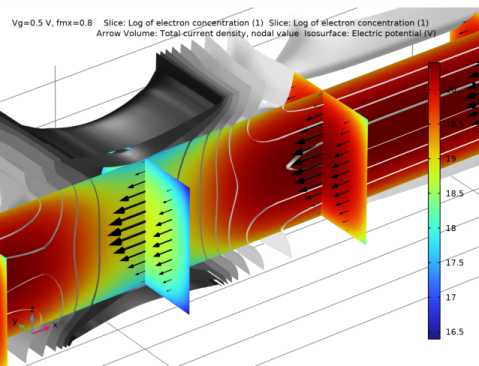
In the Settings window for Arrow Volume, click Replace Expression in the upper-right corner of the Expression section. From the menu, choose Component 1 (comp1)>Semiconductor>Currents and charge>semi.JX,...,semi.JZ - Total current density, nodal value.
3
Locate the Arrow Positioning section. Find the Y grid points subsection. In the Points text field, type 5.
4
Find the Z grid points subsection. In the Points text field, type 19.
5
Locate the Coloring and Style section. From the Color list, choose Black.
Isosurface 1
1
Right-click Electron Concentration (semi) and choose Isosurface.
2
In the Settings window for Isosurface, locate the Expression section.
3
In the Expression text field, type V.
4
Locate the Levels section. In the Total levels text field, type 10.
5
Locate the Coloring and Style section. From the Color table list, choose GrayScale.
6
Clear the Color legend check box.
Filter 1
1
Right-click Isosurface 1 and choose Filter.
2
In the Settings window for Filter, locate the Element Selection section.
3
In the Logical expression for inclusion text field, type -5e-11<y.
4
In the Electron Concentration (semi) toolbar, click  Plot.