
|
|
|
|
1
|
|
2
|
|
3
|
Click
|
|
1
|
|
2
|
|
1
|
|
2
|
In the Model Builder window, expand the Component 1 (comp1)>Semiconductor (semi) node, then click Metal Contact 2.
|
|
1
|
|
2
|
|
3
|
|
1
|
|
2
|
|
3
|
|
1
|
|
2
|
|
3
|
Click OK.
|
|
1
|
|
2
|
|
3
|
Click OK.
|
|
1
|
|
2
|
|
1
|
|
2
|
|
3
|
|
4
|
|
5
|
|
1
|
|
2
|
Find the Initial values of variables solved for subsection. From the Settings list, choose User controlled.
|
|
3
|
|
4
|
|
5
|
|
6
|
|
7
|
|
8
|
Click OK.
|
|
9
|
|
10
|
|
11
|
|
12
|
|
13
|
|
14
|
Click
|
|
1
|
|
2
|
|
3
|
|
4
|
|
5
|
Click
|
|
7
|
Locate the Physics and Variables Selection section. Select the Modify model configuration for study step check box.
|
|
8
|
In the tree, select Component 1 (Comp1)>Semiconductor (Semi)>Metal Contact 2>Harmonic Perturbation 1.
|
|
9
|
Right-click and choose Disable.
|
|
10
|
|
1
|
|
2
|
|
3
|
|
4
|
Click OK.
|
|
5
|
|
6
|
|
7
|
|
8
|
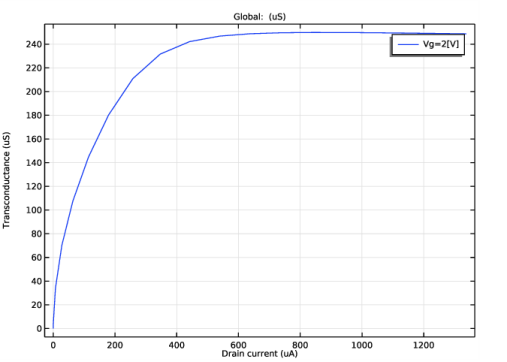
In the associated text field, type Drain current (uA).
|
|
9
|
|
10
|
In the associated text field, type Transconductance (uS).
|
|
1
|
|
2
|
|
4
|
|
5
|
|
6
|
Click Replace Expression in the upper-right corner of the x-Axis Data section. From the menu, choose Component 1 (comp1)>Semiconductor>Terminals>semi.I0_2 - Terminal current - A.
|
|
7
|
|
8
|
|
10
|
|
11
|
|
1
|
|
2
|
|
3
|
|
4
|
|
5
|
|
1
|
|
2
|
|
3
|
Click OK.
|
|
4
|
|
5
|
|
1
|
|
2
|
|
3
|
|
4
|
Click
|
|
1
|
|
2
|
|
3
|
|
4
|
|
5
|
Click
|
|
7
|
Locate the Physics and Variables Selection section. Select the Modify model configuration for study step check box.
|
|
8
|
In the tree, select Component 1 (Comp1)>Semiconductor (Semi)>Thin Insulator Gate 1>Harmonic Perturbation 1.
|
|
9
|
Right-click and choose Disable.
|
|
10
|
|
1
|
|
2
|
|
3
|
|
4
|
Click OK.
|
|
5
|
|
6
|
|
7
|
|
8
|
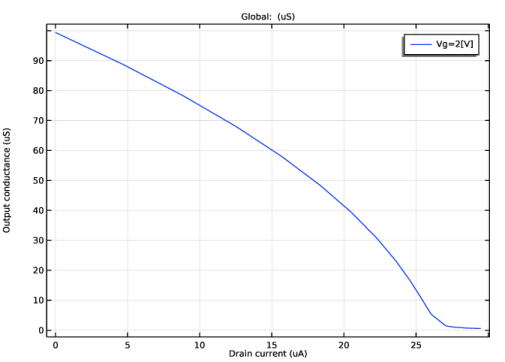
In the associated text field, type Drain current (uA).
|
|
9
|
|
10
|
In the associated text field, type Output conductance (uS).
|
|
1
|
|
2
|
|
4
|
|
5
|
|
6
|
Click Replace Expression in the upper-right corner of the x-Axis Data section. From the menu, choose Component 1 (comp1)>Semiconductor>Terminals>semi.I0_2 - Terminal current - A.
|
|
7
|
|
8
|
|
9
|
|
11
|