PDF

GaAs P-N Junction Infrared LED
This model simulates an LED that emits in the infrared part of the electromagnetic spectrum. The device structure is made up of a single p-n junction formed by a layer of p-type doping near the top surface of an otherwise n-type wafer. This kind of device geometry is simple and cheap to produce and similar LEDs are found in many household applications, for example, the IR emitters in TV remote controls. In this model the Optical Transition feature is used to calculate the electroluminescence from the device. The electronic properties are computed and the efficiency of the light production is assessed. Also, by visualizing the spacial distribution of the radiative recombination it is possible to make design suggestions to maximize the total efficiency of the output light.
Introduction
Infrared LEDs are widely used in many optoelectronic applications, but perhaps the most familiar in a household setting is for use in remote controls. Although more efficient light production can be achieved using complicated device structures, simple p-n junctions are still used for many IR emitters due to their low cost and ease of manufacture.
In this model, a simple p-n junction infrared LED is modeled. The device geometry is cylindrically symmetric, which enables a 3D visualization of the results with a much shorter computation time than would be required for a full 3D model. This model shows an example of how to use the Semiconductor Initialization study to create a refined mesh in cylindrical geometry, this is useful because this study step automatically refines the mesh around p-n junction. A second Stationary study is then used to sweep the bias applied to the device, allowing the current-voltage curve and optical emission characteristics to be calculated.
Model Definition
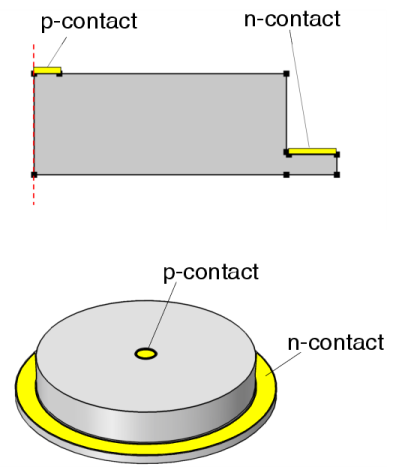
The device is made using 60 μm diameter circular chip of GaAs. Although, due to the crystalline nature of semiconductor materials, actual LED chips are likely to be fabricated using rectangular chips, only the circular active region formed by the p- and n-type doping is included in this simulation. This is in order to allow cylindrical symmetry, which considerably reduces computation time. Because the r=0 axis is an axis of symmetry, the device geometry is represented by a 30 μm wide rectangle with a thickness of 10 μm. The bottom 7.5 μm of the device are n-doped and the top 2.5 μm are p-doped. A rectangular trench has been etched down to the n-type layer at the right hand side of the domain to allow an electrical contact to be deposited onto the n-type side of the p-n junction, creating a ring of metal around the edge of the device. The p-type contact is deposited directly on the top surface in the center of the device, creating a metal disk. This configuration is shown in Figure 1.
Figure 1: Device geometry. Top: Geometry view showing one half of a 2D cross section through the diameter of the device. The axis of symmetry is shown as a red dashed line. Bottom: The 3D device geometry.
An Optical Transitions feature is added to the domain to allow the electroluminescence to be calculated. This is achieved by clearing the Stimulated Emission check box within the feature, such that only the Spontaneous Emission will be calculated. In the absence of any optical excitement from an incident electromagnetic field the spontaneous emission will be the electroluminescence due to the carrier dynamics of the injected current.
An Auger Recombination feature has been added to include a nonradiative recombination mechanism. This is only one possible nonradiative recombination mechanism, in reality a variety of other processes may be present, such as lattice/impurity scattering and phonon interactions. However, for the purpose of this demonstration model Auger recombination is sufficient to capture the important behavior that the efficiency of the radiative emission drastically reduces with increased current densities.
The model uses two studies. The first study is a Semiconductor Initialization study, which is used to automatically refine the mesh around the gradient of the dopant concentration. This is useful because the refined mesh is denser around the p-n junctions, which is where a smaller resolution is required.
The second study sweeps the voltage bias across the device from 0 V to 1.5 V. The current-voltage curve is plotted, to show that the device is indeed a diode, and the emission rate throughout the device is calculated.
Results and Discussion
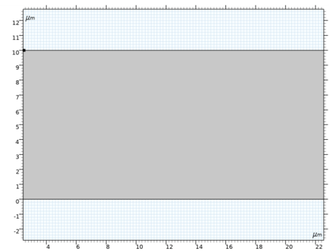
The default mesh, with the size set to Fine, is shown in Figure 2. The refined mesh, output by the first study, is shown in Figure 3 and the doping is shown in Figure 4. From these two figures it can be seen that the mesh has been refined in region of the p-n junction as desired.
Figure 2: Default physics induced mesh after the size node has been set to Finer.
Figure 3: Refined mesh output by the Semiconductor Initialization study step in the first study. The mesh density is increased in the p-n junction region.
Figure 4: Signed dopant concentration shows the p-type surface layer in blue and the n-type region in red. The doping gradually transitions from n-type to p-type over a range of a few μm to create a wide region in which light emission can occur.
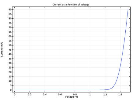
Figure 5: Current as a function of voltage showing diode behavior with a turn-on voltage just above 1.2 V.
Figure 5 shows the current as a function of the voltage bias. The device is clearly a diode, with a turn-on voltage of around 1.2 V.
Figure 6 and Figure 7 show the emission rate throughout the device for a voltage of 1.5 V and 1.2 V. At the larger bias the emission has become concentrated toward the center of the device.
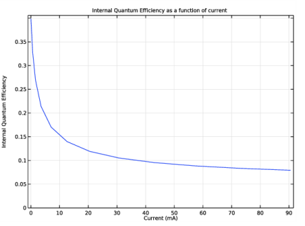
Figure 8 shows the total rate of emission, integrated over the entire domain of the device, as a function of the current. The sublinear curve is characteristic of a LED droop, a phenomenon where the efficiency of LEDs decreases with increased current density. This reduction in efficiency is even more apparent in Figure 9, which shows the Internal Quantum Efficiency (IQE) as a function of the current. The IQE is the ratio of the emission rate to the carrier injection rate, and gives the proportion of injected carriers which radiatively recombine to emit light. Initially the IQE is very low, as no current flows, however as soon as current begins to flow the IQE is initially quite high. As the current increases the IQE drops drastically to plateau at a value of 0.075. In this model, Auger recombination has been included as a nonradiative recombination mechanism. The rate of Auger recombination is proportional to the cube of the carrier density, whilst the radiative emission rate is proportional to the square of the carrier density. This means that as the carrier density is increased by the increasing current a larger proportion of the carriers recombine via the Auger mechanism, leading to the observed drastic reduction in IQE.
Figure 6: Emission rate throughout the device at a voltage bias of 1.5 V.
Figure 7: Emission rate throughout the device at a voltage bias of 1.2 V.
Figure 8: Total emission rate as a function of current. The sublinear curve is indicative of LED droop.
Figure 9: Internal Quantum Efficiency as a function of current. The drastic drop in efficiency corresponds with the sublinear increase in total emission.
The IQE is only a measure of the efficiency of the radiative recombination within the device. In order to assess the actual efficiency of the device as a light source other considerations need to be included. Specifically, it is important to consider where within the device the light is emitted from. As the p-contact on the top surface is opaque, emission underneath the p-contact may not contribute to the emitted light intensity from the device. From Figure 6 and Figure 7, which show the spacial distribution of the radiative emission, it can be seen that the emission becomes concentrated toward the center of the device with increasing voltages. This is more apparent in Figure 10, which shows a 3D visualization of the data from Figure 6. The IQE, shown in Figure 9, indicates that efficient operation of the LED would occur with low currents below 5 mA. This would be the desirable range of operation current for a remote control device, where intensity of the emission is not important compared to increased battery lifetime. These currents corresponds to voltages between 1.2 and 1.3 V and so the emission will be distributed similar to that shown in Figure 7, where the emission occurs throughout the entire p-type layer. For these voltages the position of the p-contact does not block most of the light emission from leaving the device. However, if the LED was to be used in a situation where total brightness was more important than efficiency it could be desirable to drive the device with a larger current. This could be the case if the LED was providing illumination for an infrared night-vision security camera, for example. In this case, although increasing the current increases the total rate of emission, the localization of the emission to the region underneath the p-contact could significantly reduce the total light emitted. For such a scenario it would be advantageous to change the material used for the p-contact so that it was transparent to IR light, or perhaps amened the geometry of the p-contact. For example, a ring shaped p-contact, which would allow the brightest emission on the central axis to leave the device, could be considered.
This example highlights the importance of simulation tools when designing optoelectronic semiconductor devices, as it is much cheaper to simulate several designs before committing to manufacture a device.
Figure 10: Emission rate throughout the device for an applied voltage of 1.5 V. This figure is a 3D visualization of the data in Figure 6.
Application Library path: Semiconductor_Module/Photonic_Devices_and_Sensors/gaas_pn_junction_infrared_led_diode
Modeling Instructions
From the File menu, choose New.
New
In the New window, click  Model Wizard.
Model Wizard
1
In the Model Wizard window, click  2D Axisymmetric.
2
In the Select Physics tree, select Semiconductor>Semiconductor (semi).
3
Click Add.
4
Click  Study.
5
In the Select Study tree, select Preset Studies for Selected Physics Interfaces>Semiconductor Initialization.
6
Global Definitions
Parameters 1
1
In the Model Builder window, under Global Definitions click Parameters 1.
2
In the Settings window for Parameters, locate the Parameters section.
3
Geometry 1
1
In the Model Builder window, under Component 1 (comp1) click Geometry 1.
2
In the Settings window for Geometry, locate the Units section.
3
From the Length unit list, choose µm.
Rectangle 1 (r1)
1
In the Geometry toolbar, click  Rectangle.
2
In the Settings window for Rectangle, locate the Size and Shape section.
3
In the Width text field, type w_dom.
4
In the Height text field, type h_dom.
Rectangle 2 (r2)
1
In the Geometry toolbar, click  Rectangle.
2
In the Settings window for Rectangle, locate the Size and Shape section.
3
In the Width text field, type w_con_n.
4
In the Height text field, type h_con_n.
5
Locate the Position section. In the r text field, type w_dom.
Union 1 (uni1)
1
In the Geometry toolbar, click  Booleans and Partitions and choose Union.
2
Click in the Graphics window and then press Ctrl+A to select both objects.
3
In the Settings window for Union, locate the Union section.
4
Clear the Keep interior boundaries check box.
Polygon 1 (pol1)
1
In the Geometry toolbar, click  Polygon.
2
In the Settings window for Polygon, locate the Coordinates section.
3
Fillet 1 (fil1)
1
In the Geometry toolbar, click  Fillet.
2
On the object uni1, select Point 4 only.
It might be easier to select the correct point by using the Selection List window. To open this window, in the Home toolbar click Windows and choose Selection List. (If you are running the cross-platform desktop, you find Windows in the main menu.)
3
In the Settings window for Fillet, locate the Radius section.
4
In the Radius text field, type r_fill.
5
Click  Build All Objects.
6
Click the  Zoom Extents button in the Graphics toolbar.
Add Material
1
In the Home toolbar, click  Add Material to open the Add Material window.
2
Go to the Add Material window.
3
In the tree, select Semiconductors>GaAs - Gallium Arsenide.
4
Click Add to Component in the window toolbar.
5
In the Home toolbar, click  Add Material to close the Add Material window.
Semiconductor (semi)
1
In the Model Builder window, under Component 1 (comp1) click Semiconductor (semi).
2
In the Settings window for Semiconductor, locate the Model Properties section.
3
From the Carrier statistics list, choose Fermi-Dirac.
p Doping
1
In the Physics toolbar, click  Domains and choose Analytic Doping Model.
2
In the Settings window for Analytic Doping Model, type p Doping in the Label text field.
3
Locate the Domain Selection section. From the Selection list, choose All domains.
4
Locate the Distribution section. From the list, choose Box.
5
Locate the Impurity section. In the NA0 text field, type 1e18[1/cm^3].
6
Locate the Uniform Region section. Specify the r0 vector as
7
In the W text field, type w_dom.
8
In the H text field, type h_p.
9
Locate the Profile section. From the Specify profile length scale list, choose Decay length.
10
In the ld text field, type 2[um].
n Doping
1
In the Physics toolbar, click  Domains and choose Analytic Doping Model.
2
In the Settings window for Analytic Doping Model, type n Doping in the Label text field.
3
Locate the Domain Selection section. From the Selection list, choose All domains.
4
Locate the Distribution section. From the list, choose Box.
5
Locate the Impurity section. From the Impurity type list, choose Donor doping (n-type).
6
In the ND0 text field, type 1e18[1/cm^3].
7
Locate the Uniform Region section. In the W text field, type w_dom+w_con_n.
8
In the H text field, type h_dom-h_p.
9
Locate the Profile section. From the Specify profile length scale list, choose Decay length.
10
In the ld text field, type 2[um].
p Contact
1
In the Physics toolbar, click  Boundaries and choose Metal Contact.
2
In the Settings window for Metal Contact, type p Contact in the Label text field.
3
4
Locate the Terminal section. In the V0 text field, type V_p.
n Contact
1
In the Physics toolbar, click  Boundaries and choose Metal Contact.
2
In the Settings window for Metal Contact, type n Contact in the Label text field.
3
4
Locate the Terminal section. In the V0 text field, type V_n.
Optical Transitions 1
1
In the Physics toolbar, click  Domains and choose Optical Transitions.
2
3
In the Settings window for Optical Transitions, locate the Optical Transitions section.
4
Clear the Stimulated absorption and emission check box.
Auger Recombination 1
1
In the Physics toolbar, click  Domains and choose Auger Recombination.
2
Materials
GaAs - Gallium Arsenide (mat1)
1
In the Model Builder window, under Component 1 (comp1)>Materials click GaAs - Gallium Arsenide (mat1).
2
In the Settings window for Material, locate the Material Contents section.
3
m6/s
m6/s
Add a nonlocal integration coupling for use in postprocessing the results.
Definitions (comp1)
Integration 1 (intop1)
1
In the Definitions toolbar, click  Nonlocal Couplings and choose Integration.
2
Use a semiconductor initialization study to refine the mesh.
Study 1: Mesh Refinement
1
In the Model Builder window, click Study 1.
2
In the Settings window for Study, type Study 1: Mesh Refinement in the Label text field.
3
Locate the Study Settings section. Clear the Generate default plots check box.
4
In the Home toolbar, click  Compute.
Component 1 (comp1)
Compare the two meshes, note that the refined mesh is denser around the p-n junction.
Mesh 1
1
In the Model Builder window, expand the Component 1 (comp1)>Meshes node.
2
Right-click Component 1 (comp1)>Meshes>Mesh 1 and choose Build All.
3
Click the  Zoom Extents button in the Graphics toolbar.
Level 1 Adapted Mesh 1
Click the  Zoom Extents button in the Graphics toolbar.
Before adding and configuring the main voltage sweep study, confirm the doping profile using a 2D surface plot.
Results
Doping
1
In the Home toolbar, click  Add Plot Group and choose 2D Plot Group.
2
In the Settings window for 2D Plot Group, type Doping in the Label text field.
Surface 1
1
Right-click Doping and choose Surface.
2
In the Settings window for Surface, locate the Expression section.
3
In the Expression text field, type semi.Nd-semi.Na.
4
In the Doping toolbar, click  Plot.
The doping should look like Figure 4.
Add a study to perform the voltage sweep.
Add Study
1
In the Home toolbar, click  Add Study to open the Add Study window.
2
Go to the Add Study window.
3
Find the Studies subsection. In the Select Study tree, select General Studies>Stationary.
4
Click Add Study in the window toolbar.
5
In the Home toolbar, click  Add Study to close the Add Study window.
Study 2: Voltage Sweep
1
In the Model Builder window, click Study 2.
2
In the Settings window for Study, locate the Study Settings section.
3
Clear the Generate default plots check box.
4
In the Label text field, type Study 2: Voltage Sweep.
Step 1: Stationary
1
In the Model Builder window, under Study 2: Voltage Sweep click Step 1: Stationary.
2
In the Settings window for Stationary, click to expand the Study Extensions section.
3
Select the Auxiliary sweep check box.
4
5
Solution 5 (sol5)
1
In the Study toolbar, click  Show Default Solver.
2
In the Model Builder window, expand the Solution 5 (sol5) node.
3
Right-click Study 2: Voltage Sweep>Solver Configurations>Solution 5 (sol5)>Stationary Solver 1 and choose Segregated.
4
In the Model Builder window, expand the Study 2: Voltage Sweep>Solver Configurations>Solution 5 (sol5)>Stationary Solver 1>Segregated 1 node, then click Segregated Step.
5
In the Settings window for Segregated Step, click to expand the Method and Termination section.
6
From the Nonlinear method list, choose Automatic (Newton).
7
In the Model Builder window, under Study 2: Voltage Sweep>Solver Configurations>Solution 5 (sol5)>Stationary Solver 1 right-click Segregated 1 and choose Lower Limit.
8
In the Settings window for Lower Limit, locate the Lower Limit section.
9
In the Lower limits (field variables) text field, type comp1.Ne 1 comp1.Ph 1.
10
In the Study toolbar, click  Compute.
Plot the current-voltage curve to see that the device behaves as a diode.
Results
Current vs. Voltage
1
In the Home toolbar, click  Add Plot Group and choose 1D Plot Group.
2
In the Settings window for 1D Plot Group, type Current vs. Voltage in the Label text field.
3
Locate the Data section. From the Dataset list, choose Study 2: Voltage Sweep/Solution 5 (sol5).
4
Locate the Plot Settings section. Select the x-axis label check box.
5
6
Select the y-axis label check box.
7
8
Click to expand the Title section. From the Title type list, choose Manual.
9
In the Title text area, type Current as a function of voltage.
Global 1
1
Right-click Current vs. Voltage and choose Global.
2
In the Settings window for Global, locate the y-Axis Data section.
3
4
Click to expand the Legends section. Clear the Show legends check box.
5
In the Current vs. Voltage toolbar, click  Plot.
Plot the electroluminescence emission rate throughout the device, the effects of varying the voltage can be seen by changing the value of V_p for which the results are plotted. At voltages just above the turn on voltage the emission is spread out radially but it becomes more concentrated under the central p-contact as the voltage is increased.
Emission Rate
1
In the Home toolbar, click  Add Plot Group and choose 2D Plot Group.
2
In the Settings window for 2D Plot Group, type Emission Rate in the Label text field.
3
Locate the Data section. From the Dataset list, choose Study 2: Voltage Sweep/Solution 5 (sol5).
4
Click to expand the Title section. From the Title type list, choose Manual.
5
In the Title text area, type Emission Rate.
Surface 1
1
Right-click Emission Rate and choose Surface.
2
In the Settings window for Surface, locate the Expression section.
3
In the Expression text field, type semi.ot1.R_spon.
4
In the Unit field, type 1/(cm^3*s).
5
In the Emission Rate toolbar, click  Plot.
The default plot shows the case for V_p=1.5V. However, cycling through several values of V_p allows data for other values to be viewed. This is done by selecting the desired value from the list, for example:
Emission Rate
1
In the Model Builder window, click Emission Rate.
2
In the Settings window for 2D Plot Group, locate the Data section.
3
From the Parameter value (V_p (V)) list, choose 1.2528.
4
In the Emission Rate toolbar, click  Plot.
The internal efficiency of the device can be assessed using two graphs, one that shows the total emission rate as a function of current and one that calculates the Internal Quantum Efficiency. The total emission rate can be plotted by using the integration operator to integrate the emission rate variable throughout the entire domain.
Emission Rate vs. Current
1
In the Home toolbar, click  Add Plot Group and choose 1D Plot Group.
2
In the Settings window for 1D Plot Group, type Emission Rate vs. Current in the Label text field.
3
Locate the Data section. From the Dataset list, choose Study 2: Voltage Sweep/Solution 5 (sol5).
4
Locate the Title section. From the Title type list, choose Manual.
5
In the Title text area, type Total emission rate as a function of current.
6
Locate the Plot Settings section. Select the x-axis label check box.
7
8
Select the y-axis label check box.
9
In the associated text field, type Total emission rate (1/s).
Global 1
1
Right-click Emission Rate vs. Current and choose Global.
2
In the Settings window for Global, locate the y-Axis Data section.
3
4
Locate the x-Axis Data section. From the Parameter list, choose Expression.
5
In the Expression text field, type semi.I0_1.
6
From the Unit list, choose mA.
7
Locate the Legends section. Clear the Show legends check box.
8
In the Emission Rate vs. Current toolbar, click  Plot.
The Internal Quantum Efficiency (IQE) is the proportion of injected carriers which radiatively recombine within the device. It is found by dividing the total rate of radiative transitions, calculated using the integration operator as in the previous graph, by the rate at which carriers are injected, calculated by dividing the current at the p-contact by the electron charge.
Internal Quantum Efficiency
1
In the Home toolbar, click  Add Plot Group and choose 1D Plot Group.
2
In the Settings window for 1D Plot Group, type Internal Quantum Efficiency in the Label text field.
3
Locate the Data section. From the Dataset list, choose Study 2: Voltage Sweep/Solution 5 (sol5).
4
Locate the Title section. From the Title type list, choose Manual.
5
In the Title text area, type Internal Quantum Efficiency as a function of current.
6
Locate the Plot Settings section. Select the x-axis label check box.
7
8
Select the y-axis label check box.
9
In the associated text field, type Internal Quantum Efficiency.
Remove the first few points of the voltage sweep result where the current and emission rate are too small to be computed accurately.
10
Locate the Data section. From the Parameter selection (V_p) list, choose Manual.
11
Click  Range.
12
In the Integer Range dialog box, type 5 in the Start text field.
13
In the Stop text field, type 21.
14
Click Replace.
Global 1
1
Right-click Internal Quantum Efficiency and choose Global.
2
In the Settings window for Global, locate the y-Axis Data section.
3
4
Locate the x-Axis Data section. From the Parameter list, choose Expression.
5
In the Expression text field, type semi.I0_1.
6
From the Unit list, choose mA.
7
Locate the Legends section. Clear the Show legends check box.
Internal Quantum Efficiency
1
In the Model Builder window, click Internal Quantum Efficiency.
2
In the Settings window for 1D Plot Group, locate the Axis section.
3
Select the Manual axis limits check box.
4
In the y minimum text field, type 0.
5
In the Internal Quantum Efficiency toolbar, click  Plot.
Finally, the data can be visualized in 3D due to the cylindrical symmetry. To do this, create a new dataset to hold the revolved data.
Revolution 2D 1
1
In the Results toolbar, click  More Datasets and choose Revolution 2D.
2
In the Settings window for Revolution 2D, locate the Data section.
3
From the Dataset list, choose Study 2: Voltage Sweep/Solution 5 (sol5).
4
Click to expand the Revolution Layers section. In the Start angle text field, type 270.
5
In the Revolution angle text field, type 270.
Now a 3D plot group can be used to visualize the results. By default the data is plotted for V_p = 1.5 V, however this can be changed in the same way as for the previous graphs.
Emission Rate 3D
1
In the Results toolbar, click  3D Plot Group.
2
In the Settings window for 3D Plot Group, type Emission Rate 3D in the Label text field.
3
Click to expand the Title section. From the Title type list, choose Manual.
4
In the Title text area, type Emission rate.
Volume 1
1
Right-click Emission Rate 3D and choose Volume.
2
In the Settings window for Volume, locate the Expression section.
3
In the Expression text field, type semi.ot1.R_spon.
4
In the Emission Rate 3D toolbar, click  Plot.
It is important to note that the Internal Quantum Efficiency is a metric of the efficiency of the radiative recombination within the device, and not of the actual efficiency of the output light. External factors, such as the wavelength and direction of the emission must be included when assessing the total efficiency of the device. For example, if emission is localized underneath the top p-contact then the device may not function well as the light cannot pass through the opaque metal contact.
This demonstrates both the importance of considering the entire device geometry when designing an optoelectronic device, as well as how COMSOL can be used to optimize designs. For example, for the simple device used in this model we can see from the Emission Rate versus Current graph that the total emission rate does not increase linearly with current. This is familiar behavior and is known as "LED droop". This results in the drastic drop of in efficiency with increasing current shown in the Internal Quantum Efficiency graph. However, we can also view the spacial distribution of the emission in the Emission Rate and Emission Rate 3D graphs. In these plots we see that at higher currents the emission becomes concentrated underneath the surface p-contact. This allows design changes to be made if required. For example, if efficiency was not a major concern and instead the goal was to have a high brightness then running the device with a large current could be acceptable. However, this would require either a transparent p-contact or changes to the p-contact geometry to prevent the emission from being wasted on the underside of the contact. One option which you can try is to change the p-contact geometry such that it forms a ring, if you do this and re-solve the simulation you will see that this geometry would be better for a high-brightness design.