PDF

Programming of a Floating Gate EEPROM Device
This model calculates the current and charge characteristics of a floating gate Electrically Erasable Programmable Read-Only Memory (EEPROM) device. A stationary study computes the current-voltage response of the device for a charged and uncharged floating gate. This demonstrates how the state of the memory can be read via measurements of the device resistance. Time dependent studies are then used to simulate the effects of transient voltage pulses on the control gate. These pulses cause current to tunnel between the floating gate and the semiconductor material, allowing charge to be stored or removed from the floating gate. A write-erase cycle is performed, where charge is first stored on the floating gate by an initial voltage pulse before a subsequent pulse discharges the device, returning it to its original state.
Introduction
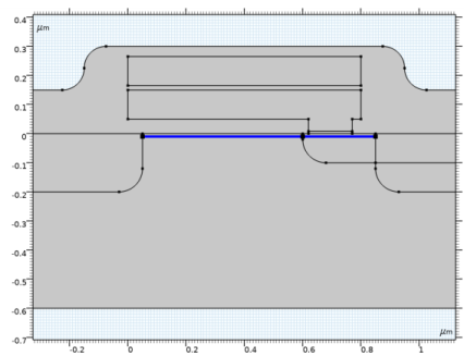
EEPROM devices are the building blocks of modern non-volatile memory, which is becoming an increasingly important storage medium for computers and mobile devices. The structure of an EEPROM device is similar to that of a MOSFET, except that the single gate contact is replaced by two electrically isolated gates: a floating gate and a control gate (see Figure 1).
Figure 1: Model geometry showing key components of the EEPROM. The tunnel barrier is highlighted in blue.
The floating gate is electrically isolated from the rest of the device and a fixed charge is applied to it, which indicates the state of the memory. During normal operation, the control gate is used in a similar manner to the gate in a MOSFET device; its potential controls the channel width. However, the field applied to the channel depends on the charge stored on the floating gate, so at a fixed control gate bias the channel resistance varies depending on the charge applied to the floating gate (see Figure 4 below).
For this device, charge is added to the floating gate (known as programming) by applying a high field to the device (hot carrier injection is also used for this process in some EEPROM devices). The geometry of the floating gate is such that the electric field is concentrated in a small region immediately over a heavily doped part of the drain contact (known as the tunnel implant). In this region the electric field exceeds the threshold for a process known as Fowler-Nordheim tunneling, in which electrons tunnel directly into the conduction band of the insulator. For the silicon-silicon oxide system only the electron tunneling is significant and the tunnel current is given by:
where Eins is the electric field in the insulator, and and are constants related to the material properties of the insulator and semiconductor (see Ref. 1 for details). As current flows into the floating gate as a result of the applied field the charge on the gate builds up and this in turn acts to oppose the applied field. Thus the charging of the floating gate is self limiting process for a fixed applied bias, similar in nature to the charging a capacitor through a resistor.
The device presented here is based on that described in Ref. 2.
Model Definition
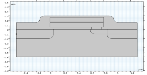
The model structure is shown in Figure 1. The device has a total length of 1.8 μm with a channel length, the distance between the highly doped n-type regions, of 0.55 μm. The source and drain contacts are 0.2 μm deep, with a shallower 0.1 μm deep tunnel implant protruding 0.25 μm from the drain region. The floating gate is separated from the channel by a 50 nm thick oxide layer, however directly above the tunnel implant the oxide thickness is only 8 nm. This 8 nm region serves a tunnel barrier between the MOSFET-like semiconductor device and the floating gate. When a voltage is applied to the control gate, the geometry of the floating gate serves to concentrate the resulting electric field in the region of the tunnel barrier. This can be seen in Figure 2, which shows the electric field during the programming voltage pulse. Sufficiently large control voltages generate an electric field capable of causing electron tunneling across the tunnel barrier.
Figure 2: Surface plot showing the electric field during the control voltage pulse used to program the EEPROM device. Note how the field is concentrated in the region of the tunnel barrier.
The first study demonstrates the effect of varying the charge stored on the floating gate. For this study, the source and base contacts are grounded and a fixed voltage of 10 mV is applied to the drain. For two different values of stored charge, 0 and -2×10-15 C, the control gate voltage is swept from 0 to 3 V. The source current is plotted as a function of the control gate voltage for both values of stored charge.
The next two studies perform a program and erase cycle. As with the first study, the source and base contacts are grounded and a fixed voltage of 10 mV is applied to the drain. A time dependent voltage pulse is applied to the control gate, this pulse has positive sign for the program event and negative sign for the erase event, as shown below in Figure 3. For the duration of the voltage pulse electrons tunnel across the tunnel barrier. The positive program pulse causes electrons to accumulate on the floating gate. The subsequent negative pulse causes these electrons to tunnel back out again returning the floating gate near to its initial zero charge configuration. Note that the program event uses a solution from the first study as the initial condition; the erase event then takes the “programmed” state from the program event study as its initial condition.
Figure 3: Time dependent control voltage pulses used for the program and erase event studies.
Results and Discussion
Figure 4 shows the current-voltage characteristics of the device for two different values of charge stored on the floating gate. As expected, the device behaves like a MOSFET, with no current flowing between the source and drain until a threshold “turn-on” control voltage is reached. This is because at the threshold voltage the electric field induces a thin inversion layer, in which the semiconductor changes from p-type to n-type, opening a conducting channel between the source and drain regions. As the control voltage increases past the threshold the width of the conducting channel increases, reducing the resistance between the source and drain contacts and allowing more current to flow for a given source-drain voltage. The stored charge changes the turn-on voltage, resulting in a different source-drain resistance for a given control voltage. By measuring the current at a given control and drain voltage it is thus possible to tell is charge is stored on the floating gate. For example, setting the control voltage to 1 V would result in no current if the device is in the erased configuration (zero stored charge) but approximately 0.5 μA if the device was charged to 1015 C.
Figure 4: Source current as a function of control voltage for a fixed drain voltage of 10 mV. The blue line shows the curve when the device is in the erased state (zero stored charge). The green line shows the curve when the device is in the programed state.
Figure 5 shows the tunnel current as a function of time throughout the program and erase events. During the program event electrons tunnel onto the floating gate, resulting in a conventional current with negative sign. When electrons tunnel back out of the floating gate during the erase event there is a positive current of equal magnitude to the program event.
Figure 6 shows the charge stored on the floating gate as a function of time throughout the program and erase events. As the charge is due to electrons tunneling through the tunnel barrier, the program event results in the accumulation of a negative charge on the floating gate and the erase event returns the charge to near zero.
Figure 5: Tunnel current as a function of time for the program and erase events.
Figure 6: Charge on the floating gate as a function of time throughout the program and erase events.
References
1. M. Lenzlinger and E. H. Snow, “Fowler-Nordheim Tunneling into Thermally Grown SiO2,” J. Applied Physics, vol. 40, no. 1, pp. 278–283, 1969.
2. A. Concannon, S. Keeney, A. Mathewson, and C. Lombardi, “Two-Dimensional Numerical Analysis of Floating-Gate EEPROM Devices,” IEEE Transactions on Electron Devices, vol. 40, no. 7, pp. 1258–1262, 1993.
Application Library path: Semiconductor_Module/Transistors/eeprom
Modeling Instructions
From the File menu, choose New.
New
In the New window, click  Model Wizard.
Model Wizard
1
In the Model Wizard window, click  2D.
2
In the Select Physics tree, select Semiconductor>Semiconductor (semi).
3
Click Add.
4
Click  Study.
5
In the Select Study tree, select General Studies>Stationary.
6
Geometry 1
For convenience, the device geometry will be inserted from an existing file. Once the geometry sequence is inserted it can be explored, in the usual way by clicking through the nodes in the Model Builder, if desired.
1
In the Geometry toolbar, click Insert Sequence and choose Insert Sequence.
2
Add a line to help make mesh later.
Line Segment 1 (ls1)
1
In the Geometry toolbar, click  More Primitives and choose Line Segment.
2
In the Settings window for Line Segment, locate the Starting Point section.
3
From the Specify list, choose Coordinates.
4
In the x text field, type 0.05.
5
In the y text field, type -0.01.
6
Locate the Endpoint section. From the Specify list, choose Coordinates.
7
In the x text field, type 0.85.
8
In the y text field, type -0.01.
9
Click  Build All Objects.
Mesh Control Edges 1 (mce1)
1
In the Geometry toolbar, click  Virtual Operations and choose Mesh Control Edges.
2
On the object fin, select Boundaries 18 and 22 only.
It might be easier to select the correct boundaries by using the Selection List window. To open this window, in the Home toolbar click Windows and choose Selection List. (If you are running the cross-platform desktop, you find Windows in the main menu.)
Add materials to the geometry, the Silicon (Si) material from the semiconductor material menu will be used for the semiconductor region and a blank material with the permittivity of Silicon Oxide (SiO2) will be used for the oxide layer.
Add Material
1
In the Home toolbar, click  Add Material to open the Add Material window.
2
Go to the Add Material window.
3
In the tree, select Semiconductors>Si - Silicon.
4
Click Add to Component in the window toolbar.
Materials
Material 2 (mat2)
1
In the Model Builder window, under Component 1 (comp1) right-click Materials and choose Blank Material.
2
3
In the Settings window for Material, locate the Material Contents section.
4
5
In the Home toolbar, click  Add Material to close the Add Material window.
Global Definitions
Enter some parameters which will be used to define the charge and voltages applied to the model.
Parameters 1
1
In the Model Builder window, under Global Definitions click Parameters 1.
2
In the Settings window for Parameters, locate the Parameters section.
3
Create the time dependent voltage pulse which will be used in the program and erase event simulations.
Rectangle 1 (rect1)
1
In the Home toolbar, click  Functions and choose Global>Rectangle.
2
In the Settings window for Rectangle, locate the Parameters section.
3
In the Lower limit text field, type 2e-6.
4
In the Upper limit text field, type 5.6e-6.
5
Click to expand the Smoothing section. In the Size of transition zone text field, type 1.6e-6.
Control voltage pulse
1
In the Model Builder window, right-click Global Definitions and choose Variables.
2
In the Settings window for Variables, locate the Variables section.
3
4
Right-click Variables 1 and choose Rename.
5
In the Rename Variables dialog box, type Control voltage pulse in the New label text field.
6
Configure the physics in the Semiconductor interface. First remove the control and floating contacts from the semiconductor interface selection. This is equivalent to assuming that they are perfect conductors.
Semiconductor (semi)
1
In the Settings window for Semiconductor, locate the Domain Selection section.
2
From the Selection list, choose Manual.
3
Add a Charge Conservation feature to the oxide layer.
Charge Conservation 1
1
Right-click Component 1 (comp1)>Semiconductor (semi) and choose the domain setting Electrostatics>Charge Conservation.
2
Next create the doping profile. The doping profile has three components: a background doping level throughout the entire semiconductor region; two doped regions, one at either side of the semiconductor region, which make up the source and drain contacts for the transistor; and a shallow doped region from which charge tunnels into the floating gate.
First apply a constant p-type background doping concentration.
Analytic Doping Model 1
1
In the Physics toolbar, click  Domains and choose Analytic Doping Model.
2
In the Settings window for Analytic Doping Model, locate the Domain Selection section.
3
From the Selection list, choose All domains.
Now create the n-type source and drain doping. Typically these doping regions would be created using an ion implantation process. This is approximated in the model by using an Analytical Doping Model feature to specify regions of constant doping and then using a Geometric Doping Model to create a Gaussian profile away from the edge of these regions.
Analytic Doping Model 2
1
In the Physics toolbar, click  Domains and choose Analytic Doping Model.
2
3
In the Settings window for Analytic Doping Model, locate the Impurity section.
4
From the Impurity type list, choose Donor doping (n-type).
5
In the ND0 text field, type 5e17[1/cm^3].
Geometric Doping Model 1
1
In the Physics toolbar, click  Domains and choose Geometric Doping Model.
2
3
In the Settings window for Geometric Doping Model, locate the Impurity section.
4
From the Impurity type list, choose Donor doping (n-type).
5
In the ND0 text field, type 5e17[1/cm^3].
6
Locate the Profile section. From the Specify profile length scale list, choose Decay length.
7
In the ld text field, type 0.02[um].
Boundary Selection for Doping Profile 1
1
In the Model Builder window, expand the Geometric Doping Model 1 node, then click Boundary Selection for Doping Profile 1.
2
Now create the doped region below the tunnel barrier into the floating contact. As this doping region is shallower than the source and drain regions it would typically be added with a second implantation process. As before, a combination of a uniform region, specified with an Analytic Doping Model, and a Gaussian profile, specified with a Geometric Doping Model, are used.
Analytic Doping Model 3
1
In the Physics toolbar, click  Domains and choose Analytic Doping Model.
2
3
In the Settings window for Analytic Doping Model, locate the Impurity section.
4
From the Impurity type list, choose Donor doping (n-type).
5
In the ND0 text field, type 1e18[1/cm^3].
Geometric Doping Model 2
1
In the Physics toolbar, click  Domains and choose Geometric Doping Model.
2
3
In the Settings window for Geometric Doping Model, locate the Impurity section.
4
From the Impurity type list, choose Donor doping (n-type).
5
In the ND0 text field, type 1e18[1/cm^3].
6
Locate the Profile section. From the Specify profile length scale list, choose Decay length.
7
In the ld text field, type 0.02[um].
Boundary Selection for Doping Profile 1
1
In the Model Builder window, expand the Geometric Doping Model 2 node, then click Boundary Selection for Doping Profile 1.
2
The boundary conditions for the semiconductor interface need to be specified, these will define the floating and control gates as well as the source and drain terminals and the tunneling barrier.
Add a Metal Contact boundary for the source.
Source
1
In the Physics toolbar, click  Boundaries and choose Metal Contact.
2
3
Right-click Metal Contact 1 and choose Rename.
4
In the Rename Metal Contact dialog box, type Source in the New label text field.
5
Add a Metal Contact boundary to ground the base of the device.
Base
1
In the Physics toolbar, click  Boundaries and choose Metal Contact.
2
3
Right-click Metal Contact 2 and choose Rename.
4
In the Rename Metal Contact dialog box, type Base in the New label text field.
5
Add a Metal Contact boundaries for the drain. Two boundary conditions are required, one for the stationary study and one for the time dependent study.
Drain (Stationary)
1
In the Physics toolbar, click  Boundaries and choose Metal Contact.
2
3
In the Settings window for Metal Contact, locate the Terminal section.
4
In the V0 text field, type Vd.
5
Right-click Metal Contact 3 and choose Rename.
6
In the Rename Metal Contact dialog box, type Drain (Stationary) in the New label text field.
7
Drain (Time Dependent)
1
In the Physics toolbar, click  Boundaries and choose Metal Contact.
2
3
In the Settings window for Metal Contact, locate the Terminal section.
4
In the V0 text field, type Vd.
5
In the Terminal name text field, type 3.
6
Right-click Metal Contact 4 and choose Rename.
7
In the Rename Metal Contact dialog box, type Drain (Time Dependent) in the New label text field.
8
Add Terminal boundary conditions to the boundaries of the control contact. Two features are required, one for the stationary study and one for the time dependent study.
Control gate (Stationary)
1
In the Physics toolbar, click  Boundaries and choose Terminal.
2
3
In the Settings window for Terminal, locate the Terminal section.
4
From the Terminal type list, choose Voltage.
5
In the V0 text field, type Vcontrol.
6
Right-click Terminal 1 and choose Rename.
7
In the Rename Terminal dialog box, type Control gate (Stationary) in the New label text field.
8
Control gate (Time Dependent)
1
In the Physics toolbar, click  Boundaries and choose Terminal.
2
3
In the Settings window for Terminal, locate the Terminal section.
4
In the Terminal name text field, type 4.
5
From the Terminal type list, choose Voltage.
6
In the V0 text field, type Vcontrol_t.
7
Right-click Terminal 2 and choose Rename.
8
In the Rename Terminal dialog box, type Control gate (Time Dependent) in the New label text field.
9
Add Insulator Tunneling boundary conditions to the boundary of the semiconductor material through which tunneling will occur.
Tunnel barrier
1
In the Physics toolbar, click  Boundaries and choose Insulator Interface.
2
3
In the Settings window for Insulator Interface, locate the Tunneling section.
4
From the Tunneling type list, choose Fowler-Nordheim tunneling.
5
Locate the Fowler-Nordheim Tunneling section. In the AnFN text field, type A_fn.
6
In the BnFN text field, type B_fn.
7
Right-click Insulator Interface 2 and choose Rename.
8
In the Rename Insulator Interface dialog box, type Tunnel barrier in the New label text field.
9
Add the Floating Gate boundary condition to the boundaries of the floating gate.
Floating Gate
1
In the Physics toolbar, click  Boundaries and choose Floating Gate.
2
3
In the Settings window for Floating Gate, locate the Floating Gate section.
4
In the Qinit text field, type Qgate.
5
Right-click Floating Gate 1 and choose Rename.
6
In the Rename Floating Gate dialog box, type Floating Gate in the New label text field.
7
Configure the mesh to be finer around the regions of interest, in particular the mesh density must be very high in the channel region under the gate and in the tunnel barrier region.
Mesh 1
Size 1
1
In the Model Builder window, under Component 1 (comp1) right-click Mesh 1 and choose Size.
2
In the Settings window for Size, locate the Geometric Entity Selection section.
3
From the Geometric entity level list, choose Domain.
4
5
Locate the Element Size section. From the Predefined list, choose Finer.
Size 2
1
In the Model Builder window, right-click Mesh 1 and choose Size.
2
In the Settings window for Size, locate the Geometric Entity Selection section.
3
From the Geometric entity level list, choose Boundary.
4
5
Locate the Element Size section. From the Calibrate for list, choose Semiconductor.
6
From the Predefined list, choose Fine.
Size 3
1
Right-click Mesh 1 and choose Size.
2
In the Settings window for Size, locate the Geometric Entity Selection section.
3
From the Geometric entity level list, choose Boundary.
4
5
Locate the Element Size section. Click the Custom button.
6
Locate the Element Size Parameters section. Select the Maximum element size check box.
7
Edge 1
1
In the Mesh toolbar, click  Edge.
2
Size 1
1
Right-click Edge 1 and choose Size.
2
In the Settings window for Size, locate the Element Size section.
3
From the Calibrate for list, choose Semiconductor.
4
From the Predefined list, choose Extra fine.
5
Click the Custom button.
6
Locate the Element Size Parameters section. Select the Maximum element size check box.
7
Size 2
1
In the Model Builder window, right-click Edge 1 and choose Size.
2
In the Settings window for Size, locate the Geometric Entity Selection section.
3
From the Geometric entity level list, choose Point.
4
5
Locate the Element Size section. From the Calibrate for list, choose Semiconductor.
6
From the Predefined list, choose Extra fine.
7
Click the Custom button.
8
Locate the Element Size Parameters section. Select the Maximum element size check box.
9
10
Select the Maximum element growth rate check box.
11
Copy Edge 1
1
In the Model Builder window, right-click Mesh 1 and choose Copying Operations>Copy Edge.
2
3
In the Settings window for Copy Edge, locate the Destination Boundaries section.
4
Click to select the  Activate Selection toggle button.
5
Copy Edge 2
1
Right-click Mesh 1 and choose Copying Operations>Copy Edge.
2
3
In the Settings window for Copy Edge, locate the Destination Boundaries section.
4
Click to select the  Activate Selection toggle button.
5
Mapped 1
1
In the Mesh toolbar, click  Mapped.
2
In the Settings window for Mapped, locate the Domain Selection section.
3
From the Geometric entity level list, choose Domain.
4
5
Click to expand the Control Entities section. Clear the Smooth across removed control entities check box.
6
Click to expand the Reduce Element Skewness section. Select the Adjust edge mesh check box.
Distribution 1
1
Right-click Mapped 1 and choose Distribution.
2
3
In the Settings window for Distribution, locate the Distribution section.
4
From the Distribution type list, choose Predefined.
5
In the Number of elements text field, type 6.
6
In the Element ratio text field, type 3.
7
From the Growth rate list, choose Exponential.
Distribution 2
1
In the Model Builder window, right-click Mapped 1 and choose Distribution.
2
Free Triangular 1
1
In the Mesh toolbar, click  Free Triangular.
2
In the Settings window for Free Triangular, locate the Domain Selection section.
3
From the Geometric entity level list, choose Domain.
4
5
Click to expand the Control Entities section. Clear the Smooth across removed control entities check box.
Information
1
In the Mesh toolbar, click  Build Mesh.
The resulting mesh is shown below.
Confirm that the doping profile is implemented as intended. This is achieved by getting the initial value from the default study settings and plotting a 2D surface plot of the net doping concentration.
Study 1
1
In the Model Builder window, click Study 1.
2
In the Settings window for Study, locate the Study Settings section.
3
Clear the Generate default plots check box.
4
In the Study toolbar, click  Get Initial Value.
Results
2D Plot Group 1
In the Home toolbar, click  Add Plot Group and choose 2D Plot Group.
Surface 1
1
Right-click 2D Plot Group 1 and choose Surface.
2
In the Settings window for Surface, locate the Expression section.
3
In the Expression text field, type semi.Ndoping.
4
In the 2D Plot Group 1 toolbar, click  Plot.
Doping
1
In the Model Builder window, right-click 2D Plot Group 1 and choose Rename.
2
In the Rename 2D Plot Group dialog box, type Doping in the New label text field.
3
The desired doping profile is shown above.
With the physics configured and doping confirmed the main studies can be performed. Set the stationary study to sweep Vcontrol from 0 to 3 V for two different values of Qgate. Note that the time dependent boundary conditions are disabled for this study.
Study 1
Step 1: Stationary
1
In the Model Builder window, under Study 1 click Step 1: Stationary.
2
In the Settings window for Stationary, locate the Physics and Variables Selection section.
3
Select the Modify model configuration for study step check box.
4
In the tree, select Component 1 (Comp1)>Semiconductor (Semi)>Drain (Time Dependent).
5
Click  Disable.
6
In the tree, select Component 1 (Comp1)>Semiconductor (Semi)>Control Gate (Time Dependent).
7
Click  Disable.
8
Click to expand the Study Extensions section. Select the Auxiliary sweep check box.
9
10
11
12
13
From the Sweep type list, choose All combinations.
14
From the Reuse solution from previous step list, choose Auto.
Adjust scaling for better convergence.
Solution 1 (sol1)
1
In the Study toolbar, click  Show Default Solver.
2
In the Model Builder window, expand the Solution 1 (sol1) node, then click Dependent Variables 1.
3
In the Settings window for Dependent Variables, locate the Scaling section.
4
From the Method list, choose None.
5
In the Model Builder window, expand the Study 1>Solver Configurations>Solution 1 (sol1)>Dependent Variables 1 node, then click Electron solution variable (comp1.Ne).
6
In the Settings window for Field, locate the Scaling section.
7
From the Method list, choose Manual.
8
In the Scale text field, type 1.0e24.
9
In the Model Builder window, under Study 1>Solver Configurations>Solution 1 (sol1)>Dependent Variables 1 click Hole solution variable (comp1.Ph).
10
In the Settings window for Field, locate the Scaling section.
11
From the Method list, choose Manual.
12
In the Scale text field, type 1.0e22.
13
In the Model Builder window, click Study 1.
14
In the Settings window for Study, type Stationary, sweep Vcontrol for fixed Qgate. in the Label text field.
15
In the Study toolbar, click  Compute.
Plot the I-V curves for each of the control voltages.
Results
Current vs. Voltage
1
In the Home toolbar, click  Add Plot Group and choose 1D Plot Group.
2
Right-click 1D Plot Group 2 and choose Rename.
3
In the Rename 1D Plot Group dialog box, type Current vs. Voltage in the New label text field.
4
Global 1
1
Right-click Current vs. Voltage and choose Global.
2
In the Settings window for Global, locate the y-Axis Data section.
3
4
Click to expand the Legends section. From the Legends list, choose Evaluated.
5
In the Legend text field, type Qgate= eval(Qgate, C) C.
Current vs. Voltage
1
In the Model Builder window, click Current vs. Voltage.
2
In the Settings window for 1D Plot Group, locate the Plot Settings section.
3
Select the x-axis label check box.
4
5
Click to expand the Title section. From the Title type list, choose Manual.
6
In the Title text area, type Source current as a function of Control Voltage.
7
Locate the Legend section. From the Position list, choose Upper left.
8
In the Current vs. Voltage toolbar, click  Plot.
Add time dependent studies to perform the program and erase simulation.
The first time dependent study performs the Program event. In this study the control voltage pulse has positive sign and electrons tunnel out of the semiconductor across the tunnel barrier, resulting in negative charge being deposited on the floating contact.
Add Study
1
In the Home toolbar, click  Add Study to open the Add Study window.
2
Go to the Add Study window.
3
Find the Studies subsection. In the Select Study tree, select General Studies>Time Dependent.
4
Click Add Study in the window toolbar.
5
In the Home toolbar, click  Add Study to close the Add Study window.
Study 2
Step 1: Time Dependent
1
In the Settings window for Time Dependent, locate the Study Settings section.
2
In the Output times text field, type range(0,0.1e-6,7e-6).
3
Click to expand the Values of Dependent Variables section. Find the Initial values of variables solved for subsection. From the Settings list, choose User controlled.
4
From the Method list, choose Solution.
5
From the Study list, choose Stationary, sweep Vcontrol for fixed Qgate., Stationary.
6
From the Parameter value (Vcontrol (V),Qgate (C)) list, choose 32: Vcontrol=0 V, Qgate=-2E-15 C.
7
Click to expand the Study Extensions section. Select the Auxiliary sweep check box.
8
9
10
11
12
13
14
In the Model Builder window, right-click Study 2 and choose Rename.
15
In the Rename Study dialog box, type Time dependent, Program event in the New label text field.
16
17
In the Settings window for Study, locate the Study Settings section.
18
Clear the Generate default plots check box.
Solution 2 (sol2)
1
In the Study toolbar, click  Show Default Solver.
2
In the Model Builder window, expand the Solution 2 (sol2) node, then click Time-Dependent Solver 1.
3
In the Settings window for Time-Dependent Solver, click to expand the Time Stepping section.
4
From the Steps taken by solver list, choose Intermediate.
5
In the Study toolbar, click  Compute.
The second time dependent study performs the Erase event. This study starts with the device in the ’programmed’ state and applies a control voltage pulse with negative sign. This causes electrons to tunnel out of the floating contact, reducing the magnitude of the floating gate charge near to zero.
Add Study
1
In the Study toolbar, click  Add Study to open the Add Study window.
2
Go to the Add Study window.
3
Find the Studies subsection. In the Select Study tree, select General Studies>Time Dependent.
4
Click Add Study in the window toolbar.
5
In the Study toolbar, click  Add Study to close the Add Study window.
Study 3
Step 1: Time Dependent
1
In the Settings window for Time Dependent, locate the Study Settings section.
2
In the Output times text field, type range(0,0.1e-6,7e-6).
3
Locate the Values of Dependent Variables section. Find the Initial values of variables solved for subsection. From the Settings list, choose User controlled.
4
From the Method list, choose Solution.
5
From the Study list, choose Time dependent, Program event, Time Dependent.
6
From the Selection list, choose Last.
7
Locate the Study Extensions section. Select the Auxiliary sweep check box.
8
9
10
11
12
13
14
In the Model Builder window, right-click Study 3 and choose Rename.
15
In the Rename Study dialog box, type Time dependent, Erase event in the New label text field.
16
17
In the Settings window for Study, locate the Study Settings section.
18
Clear the Generate default plots check box.
Solution 3 (sol3)
1
In the Study toolbar, click  Show Default Solver.
2
In the Model Builder window, expand the Solution 3 (sol3) node, then click Time-Dependent Solver 1.
3
In the Settings window for Time-Dependent Solver, locate the Time Stepping section.
4
From the Steps taken by solver list, choose Intermediate.
5
In the Study toolbar, click  Compute.
Plot the tunnel current and the charge on the floating gate as functions of time during the Program and Erase events.
Results
Tunnel Current
1
In the Home toolbar, click  Add Plot Group and choose 1D Plot Group.
2
Right-click 1D Plot Group 3 and choose Rename.
3
In the Rename 1D Plot Group dialog box, type Tunnel Current in the New label text field.
4
5
In the Settings window for 1D Plot Group, locate the Data section.
6
From the Dataset list, choose None.
7
Locate the Title section. From the Title type list, choose Manual.
8
In the Title text area, type Tunnel current as a function of time.
9
Locate the Plot Settings section. Select the x-axis label check box.
10
11
Select the y-axis label check box.
12
Global 1
1
Right-click Tunnel Current and choose Global.
2
In the Settings window for Global, locate the Data section.
3
From the Dataset list, choose Time dependent, Program event/Solution 2 (sol2).
4
Locate the y-Axis Data section. In the table, enter the following settings:
5
Locate the x-Axis Data section. From the Unit list, choose µs.
6
Locate the Legends section. From the Legends list, choose Manual.
7
Global 2
1
In the Model Builder window, right-click Tunnel Current and choose Global.
2
In the Settings window for Global, locate the Data section.
3
From the Dataset list, choose Time dependent, Erase event/Solution 3 (sol3).
4
Locate the y-Axis Data section. In the table, enter the following settings:
5
Locate the x-Axis Data section. From the Unit list, choose µs.
6
Locate the Legends section. From the Legends list, choose Manual.
7
8
In the Tunnel Current toolbar, click  Plot.
1D Plot Group 4
1
In the Home toolbar, click  Add Plot Group and choose 1D Plot Group.
2
In the Settings window for 1D Plot Group, locate the Data section.
3
From the Dataset list, choose None.
4
Locate the Title section. From the Title type list, choose Manual.
5
In the Title text area, type Floating gate charge as a function of time.
6
Locate the Plot Settings section. Select the x-axis label check box.
7
8
Select the y-axis label check box.
9
In the associated text field, type Charge on Floating Gate (pC).
Global 1
1
Right-click 1D Plot Group 4 and choose Global.
2
In the Settings window for Global, locate the Data section.
3
From the Dataset list, choose Time dependent, Program event/Solution 2 (sol2).
4
Locate the y-Axis Data section. In the table, enter the following settings:
5
Locate the x-Axis Data section. From the Unit list, choose µs.
6
Locate the Legends section. From the Legends list, choose Manual.
7
Global 2
1
Right-click Global 1 and choose Duplicate.
2
In the Settings window for Global, locate the Data section.
3
From the Dataset list, choose Time dependent, Erase event/Solution 3 (sol3).
4
Locate the Legends section. In the table, enter the following settings:
5
In the 1D Plot Group 4 toolbar, click  Plot.
Floating Gate Charge
1
In the Model Builder window, right-click 1D Plot Group 4 and choose Rename.
2
In the Rename 1D Plot Group dialog box, type Floating Gate Charge in the New label text field.
3