PDF

A Solar Cell with InAs Quantum Dots Embedded in AlGaAs/GaAs Quantum Wells
This example shows an approximate approach to model a dot-in-well solar cell as described by Asahi et al. in the reference paper. The quantum wells and the layers of quantum dots are each treated as lumped energy levels in the bandgap. The authors specify transitions between the dot/well levels and the energy bands. The continuum part of the current density is otherwise unimpeded by the wells and dots. This description is equivalent to the trapping feature in the Semiconductor interface, so it is used to model the wells and dots in this example. The computed trend of the photocurrent and occupancy of the quantum dot states agrees well with the result shown in the paper.
Introduction
In Ref. 1, Asahi et al. studied the photocurrent generation process in a dot-in-well solar cell by shining two lasers at different wavelengths to look at the two-step photon absorption in the device. The solar cell is composed of an Al0.3Ga0.7As p-i-n structure. The intrinsic region contains in addition 10 repeating units, with each unit consisting of a GaAs quantum well (QW) and a layer of InAs quantum dots (QD) embedded in the QW. The authors observed a saturation behavior of the photocurrent with respect to the laser intensities, and used a simple model to explain this behavior. Here we show how this kind of model can be built using the Semiconductor Module.
Model Definition
The authors’ modeling approach is to treat the QW and QD as lumped energy levels. The transitions between these levels and the conduction/valence bands are described with simple lifetimes or rates in an unidirectional fashion (no detailed balancing). Other than these transitions, the current flow in the energy bands is not affected by the QW and QD. There is also a transition from the QW to the QD specified by the authors. See Fig. 6 in Ref. 1 for a summary of their model.
This description of the system is essentially the same as considering, in the Semiconductor interface, a bulk Al0.3Ga0.7As p-i-n structure with some layers of traps in the intrinsic region, where the trap energy levels represent the layers of QW and QD. The unidirectional transitions can be implemented by setting the Carrier Capture probabilities to zeros and using the Additional Carrier Capture Rate option to specify the unidirectional rates. The transition from the QW to the QD can be implemented using the Transition Between Discrete Levels feature. To minimize the reverse transition from the QD to the QW, a large energy difference between the two trap levels are used.
For simplicity, only two repeating units are implemented in this example. Additional substrate buffer layers are also neglected. The default mesh is modified to use coarser spacing in regions with very small gradients, in order to minimize round-off error. In Study 1, the double dogleg nonlinear method is used to help convergence.
See the comments in the section Modeling Instructions for more detailed discussions on the model construction, solution processes, and result visualization.
Results and Discussion
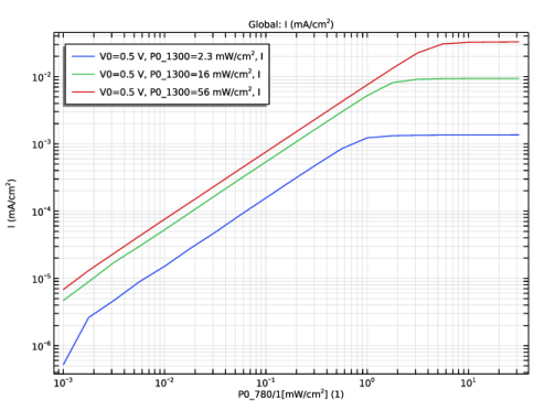
Figure 1 shows the photocurrent as a function of the 780 nm light while keeping the 1300 nm light at a few fixed values, to be compared with Fig. 7(a) in Ref. 1. The qualitative trend of saturation occurring at higher intensity of 780 nm light for higher level of 1300 nm light is well reproduced.
Figure 1: Photocurrent as a function of the 780 nm light while keeping the 1300 nm light at a few fixed values.
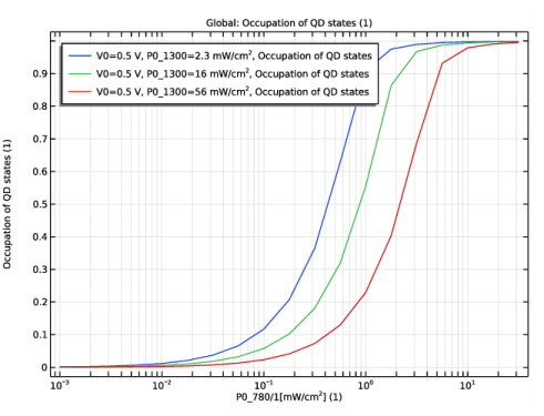
Figure 2 plots the occupancy of the QD states corresponding to the conditions shown in Figure 1, to be compared with Fig. 7(b) in Ref. 1. The qualitative trend is also well reproduced.
Figure 2: Occupancy of the QD states corresponding to the conditions shown in Figure 1.
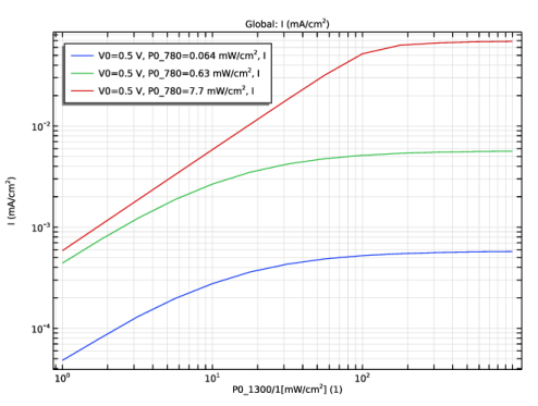
Figure 3 shows the photocurrent as a function of the 1300 nm light while keeping the 780 nm light at a few fixed values, to be compared with Fig. 7(c) in Ref. 1. The qualitative trend is also well reproduced.
Figure 3: Photocurrent as a function of the 1300 nm light while keeping the 780 nm light at a few fixed values.
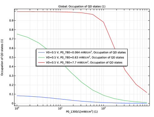
Figure 4 plots the occupancy of the QD states corresponding to the conditions shown in Figure 3, to be compared with Fig. 7(d) in Ref. 1. The qualitative trend is also well reproduced.
Figure 4: Occupancy of the QD states corresponding to the conditions shown in Figure 3.
 
References
1. S. Asahi, H. Teranishi, N. Kasamatsu, T. Kada, T. Kaizu and T. Kita, "Saturable Two-Step Photocurrent Generation in Intermediate-Band Solar Cells Including InAs Quantum Dots Embedded in Al$_{0.3}$Ga$_{0.7}$ As/GaAs Quantum Wells," in IEEE Journal of Photovoltaics, vol. 6, no. 2, pp. 465-472, March 2016, doi: 10.1109/JPHOTOV.2015.2504796.
Application Library path: Semiconductor_Module/Photonic_Devices_and_Sensors/dot_in_well_solar_cell
Modeling Instructions
From the File menu, choose New.
New
In the New window, click  Model Wizard.
Model Wizard
1
In the Model Wizard window, Use 1D geometry to model the dot-in-well solar cell.
2
3
In the Select Physics tree, select Semiconductor>Semiconductor (semi).
4
Click Add.
5
Click  Study.
It is usually a good practice to start the first study with a Semiconductor Equilibrium study step, which is easier to converge and provides a good initial condition for subsequent study steps.
6
In the Select Study tree, select Preset Studies for Selected Physics Interfaces>Semiconductor Equilibrium.
7
Geometry 1
Set the length unit to a convenient one, in this model, nanometer.
1
In the Model Builder window, under Component 1 (comp1) click Geometry 1.
2
In the Settings window for Geometry, locate the Units section.
3
From the Length unit list, choose nm.
Global Definitions
Parameters 1 - Geometry & QW, QD
Enter model parameters in a few Parameters node, first, for the geometry and the quantum well (QW) and quantum dot (QD). Hide these parameters from the Auxiliary sweep parameter drop-down menu.
1
In the Model Builder window, under Global Definitions click Parameters 1.
2
In the Settings window for Parameters, type Parameters 1 - Geometry & QW, QD in the Label text field.
3
Click to expand the Visibility section. Clear the Show in parameter selections check box.
In this example, the QW and QD are modeled as trap levels, to match the simulation approach taken by the authors of the reference paper. Following that approach, where the QW and QD are considered "lumped" energy levels, the trap levels of the QW and QD will have the same spatial extent in this model, given by the parameter t_well. The parameter t_dot will only be used for optical absorption calculations. The transition from QW to QD is considered unidirectional (no excitation from QD to QW) in the paper. To achieve this effect, an arbitrary large energy gap of 600 meV is used to separate the corresponding trap levels in this model, in the definition of the parameter DeltaE_dot Some parameters are not specified in the paper and guess values are used and indicated in the descriptions.
4
Locate the Parameters section. In the table, enter the following settings:
Parameters 2 - Swept
1
In the Home toolbar, click  Parameters and choose Add>Parameters.
Enter the parameters that will be used in the Auxiliary sweep.
2
In the Settings window for Parameters, type Parameters 2 - Swept in the Label text field.
3
Locate the Parameters section. In the table, enter the following settings:
Parameters 3 - Optical
1
In the Home toolbar, click  Parameters and choose Add>Parameters.
Enter the parameters for optical transitions and also hide them from the Auxiliary sweep parameter drop-down menu.
2
In the Settings window for Parameters, type Parameters 3 - Optical in the Label text field.
3
Locate the Visibility section. Clear the Show in parameter selections check box.
4
Locate the Parameters section. In the table, enter the following settings:
Build the geometry with 2 repeating units of the dot-in-well structure. There are 10 repeating units in the paper. In this model we illustrate the procedure with 2 units. Some of the substrate layers are also neglected for simplicity.
Geometry 1
Interval 1 - Top
1
In the Model Builder window, under Component 1 (comp1) right-click Geometry 1 and choose Interval.
2
In the Settings window for Interval, type Interval 1 - Top in the Label text field.
3
Locate the Interval section. From the Specify list, choose Interval lengths.
4
In the Left endpoint text field, type -150-540.
5
Interval 2 - 1st unit
1
In the Model Builder window, right-click Geometry 1 and choose Interval.
2
In the Settings window for Interval, type Interval 2 - 1st unit in the Label text field.
3
Locate the Interval section. In the table, enter the following settings:
4
Locate the Selections of Resulting Entities section. Find the Cumulative selection subsection. Click New.
5
In the New Cumulative Selection dialog box, type 1st unit in the Name text field.
6
Array 1 - all units
1
Right-click Geometry 1 and choose Transforms>Array.
2
In the Settings window for Array, type Array 1 - all units in the Label text field.
3
Locate the Input section. From the Input objects list, choose 1st unit.
4
Locate the Size section. In the Size text field, type 2.
5
Locate the Displacement section. In the x text field, type t_unit.
Interval 3 - Bottom
1
Right-click Geometry 1 and choose Interval.
2
In the Settings window for Interval, type Interval 3 - Bottom in the Label text field.
3
Locate the Interval section. From the Specify list, choose Interval lengths.
4
In the Left endpoint text field, type 2*t_unit.
5
6
Click  Build All Objects.
7
Click the  Zoom Extents button in the Graphics toolbar.
Add AlGaAs material from the built-in library and set the Al mole fraction to 0.3.
Add Material
1
In the Home toolbar, click  Add Material to open the Add Material window.
2
Go to the Add Material window.
3
In the tree, select Semiconductors>Al(x)Ga(1-x)As - Aluminium Gallium Arsenide.
4
Click Add to Component in the window toolbar.
5
In the Home toolbar, click  Add Material to close the Add Material window.
Materials
Al(x)Ga(1-x)As - Aluminium Gallium Arsenide (mat1)
1
In the Settings window for Material, locate the Material Contents section.
2
Find the Local properties subsection. In the table, enter the following settings:
Define domain selections for the QW and QD to be used later.
Definitions
1st well/dot
1
In the Definitions toolbar, click  Explicit.
2
In the Settings window for Explicit, type 1st well/dot in the Label text field.
3
2nd well/dot
1
In the Definitions toolbar, click  Explicit.
2
In the Settings window for Explicit, type 2nd well/dot in the Label text field.
3
all wells/dots
1
In the Definitions toolbar, click  Union.
2
In the Settings window for Union, type all wells/dots in the Label text field.
3
Locate the Input Entities section. Under Selections to add, click  Add.
4
In the Add dialog box, select 1st well/dot in the Selections to add list.
5
6
In the Settings window for Union, locate the Input Entities section.
7
Under Selections to add, click  Add.
8
In the Add dialog box, select 2nd well/dot in the Selections to add list.
9
Set up doping, metal contacts, and discrete trap energy levels representing the QW and QD. Use the Transition Between Discrete Levels feature for the transition from the QW to the QD. Use the "Additional carrier capture rate" option for other transitions. This option is more convenient for arbitrary unidirectional transitions as those adopted in the paper.
Semiconductor (semi)
1
In the Model Builder window, under Component 1 (comp1) click Semiconductor (semi).
2
In the Settings window for Semiconductor, locate the Cross-Section Area section.
3
In the A text field, type area.
Analytic Doping Model 1
1
In the Physics toolbar, click  Domains and choose Analytic Doping Model.
2
3
In the Settings window for Analytic Doping Model, locate the Impurity section.
4
In the NA0 text field, type 2e18[1/cm^3].
Analytic Doping Model 2
1
In the Physics toolbar, click  Domains and choose Analytic Doping Model.
2
3
In the Settings window for Analytic Doping Model, locate the Impurity section.
4
From the Impurity type list, choose Donor doping (n-type).
5
In the ND0 text field, type 5e16[1/cm^3].
Metal Contact 1
1
In the Physics toolbar, click  Boundaries and choose Metal Contact.
2
Metal Contact 2
1
In the Physics toolbar, click  Boundaries and choose Metal Contact.
2
3
In the Settings window for Metal Contact, locate the Terminal section.
4
In the V0 text field, type V0.
Trap-Assisted Recombination 1
1
In the Physics toolbar, click  Domains and choose Trap-Assisted Recombination.
2
In the Settings window for Trap-Assisted Recombination, locate the Domain Selection section.
3
From the Selection list, choose all wells/dots.
4
Locate the Trap-Assisted Recombination section. From the Trapping model list, choose Explicit trap distribution.
5
Locate the Trapping section. Select the Specify trap species check box.
Discrete Energy Level - wells
1
In the Physics toolbar, click  Attributes and choose Discrete Energy Level.
2
In the Settings window for Discrete Energy Level, type Discrete Energy Level - wells in the Label text field.
3
Locate the Trap Type section. From the Trap type list, choose Neutral electron traps.
4
Locate the Traps section. In the Nt,ne text field, type N_well.
5
From the Impurity energy level list, choose From conduction band edge.
6
In the Et,0 text field, type DeltaE_well.
7
In the gD text field, type gD.
8
Locate the Carrier Capture section. From the Probability of electron capture list, choose User defined. In the Cn text field, type 0.
9
From the Probability of hole capture list, choose User defined. In the Cp text field, type 0.
Discrete Energy Level - dots
1
Right-click Discrete Energy Level - wells and choose Duplicate.
2
In the Settings window for Discrete Energy Level, type Discrete Energy Level - dots in the Label text field.
3
Locate the Traps section. In the Nt,ne text field, type N_dot.
4
In the Et,0 text field, type DeltaE_dot.
Before continuing the physics setup, define variables for the QW and QD populations and transition rates. First define two integration operators over the domain of the two QW/QD. Then define 3 sets of variables.
Definitions
Integration - 1st well/dot
1
In the Definitions toolbar, click  Nonlocal Couplings and choose Integration.
2
In the Settings window for Integration, type Integration - 1st well/dot in the Label text field.
3
Locate the Source Selection section. From the Selection list, choose 1st well/dot.
Integration - 2nd well/dot
1
In the Definitions toolbar, click  Nonlocal Couplings and choose Integration.
2
In the Settings window for Integration, type Integration - 2nd well/dot in the Label text field.
3
Locate the Source Selection section. From the Selection list, choose 2nd well/dot.
Variables - all wells/dots
1
In the Model Builder window, right-click Definitions and choose Variables.
2
In the Settings window for Variables, type Variables - all wells/dots in the Label text field.
3
Locate the Geometric Entity Selection section. From the Geometric entity level list, choose Domain.
4
From the Selection list, choose all wells/dots.
5
Locate the Variables section. In the table, enter the following settings:
Variables - 1st well/dot
1
Right-click Definitions and choose Variables.
2
In the Settings window for Variables, type Variables - 1st well/dot in the Label text field.
3
Locate the Geometric Entity Selection section. From the Geometric entity level list, choose Domain.
4
From the Selection list, choose 1st well/dot.
5
Locate the Variables section. In the table, enter the following settings:
Variables - 2nd well/dot
1
Right-click Definitions and choose Variables.
2
In the Settings window for Variables, type Variables - 2nd well/dot in the Label text field.
3
Locate the Geometric Entity Selection section. From the Geometric entity level list, choose Domain.
4
From the Selection list, choose 2nd well/dot.
5
Locate the Variables section. In the table, enter the following settings:
Finish setting up the physics. Be careful about the signs of the additional carrier capture rates: the additional electron capture rate is positive for a transition of an electron from the conduction band to the trap level, and the additional hole capture rate is positive for a transition of an electron from the trap level to the valence band.
Semiconductor (semi)
Discrete Energy Level - wells
1
In the Model Builder window, under Component 1 (comp1)>Semiconductor (semi)>Trap-Assisted Recombination 1 click Discrete Energy Level - wells.
2
In the Settings window for Discrete Energy Level, click to expand the Additional Carrier Capture Rate section.
3
In the Rn,extra text field, type -n_well/tau_thermal+gamma*semi.N.
4
In the Rp,extra text field, type -G_780+n_well/tau_well.
Discrete Energy Level - dots
1
In the Model Builder window, click Discrete Energy Level - dots.
2
In the Settings window for Discrete Energy Level, locate the Additional Carrier Capture Rate section.
3
In the Rn,extra text field, type -G_1300.
4
In the Rp,extra text field, type n_dot/tau_dot.
Trap-Assisted Recombination 1
In the Model Builder window, click Trap-Assisted Recombination 1.
Transition Between Discrete Levels 1
1
In the Physics toolbar, click  Attributes and choose Transition Between Discrete Levels.
2
In the Settings window for Transition Between Discrete Levels, locate the Transition Between Discrete Levels section.
3
From the Upper level (2) list, choose Discrete Energy Level - wells.
4
From the Lower level (1) list, choose Discrete Energy Level - dots.
5
In the τ21 text field, type tau_welltodot.
Modify the default mesh to use coarser spacing in regions with very small gradients, in order to minimize round-off error.
Mesh 1
Size
In the Model Builder window, under Component 1 (comp1) right-click Mesh 1 and choose Edit Physics-Induced Sequence.
Size 1
Select Boundaries 2–8 only.
Size 2
1
Right-click Component 1 (comp1)>Mesh 1>Size 1 and choose Duplicate.
2
Right-click Size 2 and choose Move Up.
3
In the Settings window for Size, locate the Geometric Entity Selection section.
4
From the Geometric entity level list, choose Domain.
5
6
Locate the Element Size section. From the Predefined list, choose Extra coarse.
7
Click  Build All.
In study 1, ramp up the bias voltage V0 from 0 to 0.5 V, while keeping the lights off. Sometimes the double dogleg nonlinear method works better than the Newton method.
Study 1 - ramp V0 from 0 to 0.5 V, no light
1
In the Model Builder window, click Study 1.
2
In the Settings window for Study, type Study 1 - ramp V0 from 0 to 0.5 V, no light in the Label text field.
Stationary
1
In the Study toolbar, click  Study Steps and choose Stationary>Stationary.
2
In the Settings window for Stationary, click to expand the Study Extensions section.
3
Select the Auxiliary sweep check box.
4
5
Solution 1 (sol1)
1
In the Study toolbar, click  Show Default Solver.
2
In the Model Builder window, expand the Solution 1 (sol1) node.
3
In the Model Builder window, expand the Study 1 - ramp V0 from 0 to 0.5 V, no light>Solver Configurations>Solution 1 (sol1)>Stationary Solver 1 node, then click Fully Coupled 1.
4
In the Settings window for Fully Coupled, click to expand the Method and Termination section.
5
From the Nonlinear method list, choose Double dogleg.
6
Click  Compute.
Group the plots by study.
Results
Carrier Concentrations (semi), Electric Potential (semi), Energy Levels (semi)
1
In the Model Builder window, under Results, Ctrl-click to select Energy Levels (semi), Carrier Concentrations (semi), and Electric Potential (semi).
2
Study 1
In the Settings window for Group, type Study 1 in the Label text field.
Create a new study to ramp the 780 nm light while keeping the 1300 nm light at a few fixed values. Set the bias voltage at the operating point of 0.5 V, and use the corresponding solution from Study 1 as the initial condition.
Add Study
1
In the Study toolbar, click  Add Study to open the Add Study window.
2
Go to the Add Study window.
3
Find the Studies subsection. In the Select Study tree, select General Studies>Stationary.
4
Click Add Study in the window toolbar.
5
In the Study toolbar, click  Add Study to close the Add Study window.
Study 2
Step 1: Stationary
1
In the Settings window for Stationary, locate the Study Extensions section.
2
Select the Auxiliary sweep check box.
3
From the Sweep type list, choose All combinations.
4
5
6
7
8
9
10
Click to expand the Values of Dependent Variables section. Find the Initial values of variables solved for subsection. From the Settings list, choose User controlled.
11
From the Method list, choose Solution.
12
From the Study list, choose Study 1 - ramp V0 from 0 to 0.5 V, no light, Stationary.
13
From the Parameter value (V0 (V)) list, choose 0.5 V.
14
In the Model Builder window, click Study 2.
15
In the Settings window for Study, type Study 2 - ramp P_780 in the Label text field.
16
In the Study toolbar, click  Compute.
Group the plots by study. Create plots to compare with Fig. 7 (a) and (b) in the reference paper. The qualitative trend of the photo current and the occupation of QD states is well reproduced. (The current density with P_1300 off is visually much smaller than any of the values with P_1300 on. Therefore plotting those values "I" is sufficient, even though the paper plots the difference "Delta I".)
Results
Carrier Concentrations (semi) 1, Electric Potential (semi) 1, Energy Levels (semi) 1
1
In the Model Builder window, under Results, Ctrl-click to select Energy Levels (semi) 1, Carrier Concentrations (semi) 1, and Electric Potential (semi) 1.
2
Study 2
In the Settings window for Group, type Study 2 in the Label text field.
I vs. P_780 (Fig. 7a)
1
In the Home toolbar, click  Add Plot Group and choose 1D Plot Group.
2
In the Settings window for 1D Plot Group, type I vs. P_780 (Fig. 7a) in the Label text field.
3
Locate the Data section. From the Dataset list, choose Study 2 - ramp P_780/Solution 3 (sol3).
4
From the Parameter selection (P0_1300) list, choose Manual.
5
In the Parameter indices (1-4) text field, type 2 3 4.
6
Locate the Axis section. Select the x-axis log scale check box.
7
Select the y-axis log scale check box.
8
Locate the Legend section. From the Position list, choose Upper left.
Global 1
1
In the I vs. P_780 (Fig. 7a) toolbar, click  Global.
2
In the Settings window for Global, locate the y-Axis Data section.
3
4
Locate the x-Axis Data section. From the Parameter list, choose Expression.
5
In the Expression text field, type P0_780/1[mW/cm^2].
6
In the I vs. P_780 (Fig. 7a) toolbar, click  Plot.
ft_dot vs. P_780 (Fig. 7b)
1
In the Model Builder window, right-click I vs. P_780 (Fig. 7a) and choose Duplicate.
2
In the Settings window for 1D Plot Group, type ft_dot vs. P_780 (Fig. 7b) in the Label text field.
3
Locate the Axis section. Clear the y-axis log scale check box.
Global 1
1
In the Model Builder window, expand the ft_dot vs. P_780 (Fig. 7b) node, then click Global 1.
2
In the Settings window for Global, locate the y-Axis Data section.
3
4
In the ft_dot vs. P_780 (Fig. 7b) toolbar, click  Plot.
Create another new study to ramp the 1300 nm light while keeping the 780 nm light at a few fixed values. Set the bias voltage at the operating point of 0.5 V, and use the corresponding solution from Study 1 as the initial condition.
Add Study
1
In the Home toolbar, click  Add Study to open the Add Study window.
2
Go to the Add Study window.
3
Find the Studies subsection. In the Select Study tree, select Empty Study.
4
Click Add Study in the window toolbar.
5
In the Home toolbar, click  Add Study to close the Add Study window.
Study 2 - ramp P_780
Step 1: Stationary
In the Model Builder window, under Study 2 - ramp P_780 right-click Step 1: Stationary and choose Copy.
Study 3 - ramp P_1300
1
In the Model Builder window, click Study 3.
2
In the Settings window for Study, type Study 3 - ramp P_1300 in the Label text field.
3
Right-click Study 3 - ramp P_1300 and choose Paste Stationary.
Step 1: Stationary
1
In the Settings window for Stationary, locate the Study Extensions section.
2
3
Click  Move Up.
4
5
In the Home toolbar, click  Compute.
Group the plots by study. Create plots to compare with Fig. 7 (c) and (d) in the reference paper. The qualitative trend of the photo current and the occupation of QD states is well reproduced.
Results
Carrier Concentrations (semi) 2, Electric Potential (semi) 2, Energy Levels (semi) 2
1
In the Model Builder window, under Results, Ctrl-click to select Energy Levels (semi) 2, Carrier Concentrations (semi) 2, and Electric Potential (semi) 2.
2
Study 3
In the Settings window for Group, type Study 3 in the Label text field.
I vs. P_780 (Fig. 7a)
In the Model Builder window, under Results>Study 2 right-click I vs. P_780 (Fig. 7a) and choose Copy.
I vs. P_1300 (Fig. 7c)
1
In the Model Builder window, right-click Study 3 and choose Paste 1D Plot Group.
2
In the Settings window for 1D Plot Group, type I vs. P_1300 (Fig. 7c) in the Label text field.
3
Locate the Data section. From the Parameter selection (P0_1300) list, choose All.
4
From the Dataset list, choose Study 3 - ramp P_1300/Solution 4 (sol4).
Global 1
1
In the Model Builder window, expand the I vs. P_1300 (Fig. 7c) node, then click Global 1.
2
In the Settings window for Global, locate the x-Axis Data section.
3
In the Expression text field, type P0_1300/1[mW/cm^2].
4
In the I vs. P_1300 (Fig. 7c) toolbar, click  Plot.
ft_dot vs. P_780 (Fig. 7b)
In the Model Builder window, under Results>Study 2 right-click ft_dot vs. P_780 (Fig. 7b) and choose Copy.
ft_dot vs. P_1300 (Fig. 7d)
1
In the Model Builder window, right-click Study 3 and choose Paste 1D Plot Group.
2
In the Settings window for 1D Plot Group, type ft_dot vs. P_1300 (Fig. 7d) in the Label text field.
3
Locate the Data section. From the Parameter selection (P0_1300) list, choose All.
4
From the Dataset list, choose Study 3 - ramp P_1300/Solution 4 (sol4).
5
Locate the Legend section. From the Position list, choose Center.
Global 1
1
In the Model Builder window, expand the ft_dot vs. P_1300 (Fig. 7d) node, then click Global 1.
2
In the Settings window for Global, locate the x-Axis Data section.
3
In the Expression text field, type P0_1300/1[mW/cm^2].
4
In the ft_dot vs. P_1300 (Fig. 7d) toolbar, click  Plot.