PDF

Bipolar Transistor
This model shows how to set up a simple n-p-n bipolar transistor simulation. For this particular model, the current voltage characteristics in the static common-emitter configuration are computed and the common emitter current gain is determined.
Introduction
The invention of the Bipolar Transistor at Bell labs in the late 1940s was arguably the most significant technological development of the 20th century. Bipolar transistors were the workhorses of the first integrated circuits and consequently have had an enormous impact on the modern world. Although bipolar transistors have largely been replaced by field-effect devices in modern integrated circuits, they are still important, particularly in high-frequency applications.
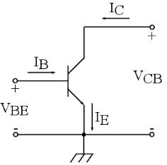
The bipolar transistor is basically a three-terminal device whose resistance between two terminals is controlled by the third. In this example, we are going to show the static characteristics of a n-p-n bipolar transistor in common-emitter mode — that is, when the base and collector voltages are measured relative to the grounded emitter. Figure 1 shows the biasing configuration of a n-p-n transistor in this configuration.
Figure 1: A n-p-n transistor in common-emitter configuration.
In the common-emitter mode, the base terminal of the transistor serves as the input, the collector is the output, and the emitter is common to both (in our case grounded). N-p-n transistors in common-emitter configuration give an inverted output and can have a high gain which is a strong function of the base current.
The model presented here shows how to perform a detailed characterization of a bipolar transistor in the common-emitter configuration.
Model Definition
The structure is half of the cross section of a simplified n-p-n bipolar transistor; see Figure 2. The model uses the following dimensions: an emitter contact length of 1.2/2 μm, a base contact length of 0.3 μm separated from the emitter contact by 0.35 μm, and a collector contact length of 2.5/2 μm. The total depth of the transistor is 1 μm with a width of 2.5/2 μm. The modeled doping profile is shown in Figure 2. As is typical of the profile used in silicon bipolar transistors, it consists of four regions (n+, p, n and n+) described in detail in Modeling Instructions.
.
Figure 2: Top: The cross-section of the modeled transistor. The differently doped regions are labeled. The red line shows the axis of symmetry used to simplified the model geometry. Bottom: A line graph, taken along the axis of symmetry, showing the doping concentration. The labeled regions (n+, n, p) correspond with those in the geometry cross-section.
This model uses several studies to characterize the DC response of the bipolar transistor current output under both voltage and current driven configurations. A Semiconductor Initialization study step is also used, which automatically refines the default mesh where the gradient of the semiconductor doping profile is large. The refined mesh is then used throughout the rest of the modeling sequence.
First, a study sweeps the base voltage with a fixed collector voltage. This allows the currents at all three terminals to be plotted as a function of VBE and demonstrates that the simulation conserves current. This study is also used to create a Gummel plot, which shows the current at the collector and base contacts as a function of the base voltage. The same data is then used to calculate the current gain, defined as the ratio of the collector and base currents (IC/IE), as a function of the collector current. The current gain curve is an important characteristic for current regulation and power control applications, as it is used to calculate the expected collector output for a given base input.
The remaining studies are used to calculate the collector current as a function of the collector voltage for two different values for the base current. This is achieved using two studies that sweep the collector voltage, one with a fixed base current of IB = 2 μA and one with a fixed base current of IB = 10 μA. These simulations are current driven because they are performed with a set base current applied. When solving current driven problems in COMSOL it is often necessary to provide an initial condition which is calculated from a suitable voltage driven study. In order to generate the required initial conditions for these studies a voltage driven initialization study is performed. This initialization study sets the collector voltage to 0, which is the initial value it has in the current driven studies, and sweeps the base voltage. The solution which generates base currents closest to 2 μA is then used as the initial condition for the collector voltage sweeps.
Results and Discussion
Figure 3 displays the current at each terminal as a function of the base-emitter voltage (VBE) for a fixed collector-emitter voltage (VCE =0.5 V). Note that the figure shows the terminal currents using the software’s sign convention: outward current from the semiconductor material is positive and inward current is negative. The figure also shows that the current is conserved. This can be seen as the difference between the emitter and collector currents, represented as magenta circles, matches the base current, shown in green. Thus the current is conserved, as
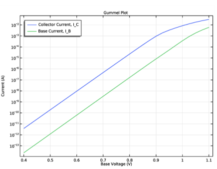
Figure 4 shows the Gummel plot for the modeled bipolar transistor. The Gummel plot shows the magnitude of the collector and base currents, plotted on a logarithmic scale, as a function of the base voltage.
Figure 5 shows current gain, defined as IC/IB, as a function of the collector current at a fixed base voltage of VBE = 0.5 V.
Figure 6 shows the collector current as a function of collector voltage for two different values of base current. This figure shows how a small base current can be used to control a larger collector current by changing the resistance between the emitter and collector terminals.
Figure 7 shows the voltage and carrier current densities throughout the device. With VCE = 1.5 V the device is in the forward-active regime. In this regime the emitter-base junction is forward biased and the base-collector junction is reverse biased. Electrons are injected from the emitter into the base through the forward biased junction. These electrons then diffuse through the p-type base region as minority carriers. Those that make it to the reverse biased base-collector junction are swept toward the collector terminal by the junction electric field. The thickness of the base region must be small enough to allow the electrons to diffuse through with high probability. Holes can travel easily from the base to the emitter regions through the forward biased emitter-base junction, but they cannot traverse the reverse biased base-collector junction. Hence the hole current flows between the emitter and base terminals without entering the lower n-doped region, and the electron current flows between the emitter and collector terminals.
Figure 3: Terminal currents as a function of the base-emitter voltage (VBE) for a fixed collector-emitter voltage (VCE = 0.5 V).
Figure 4: Gummel plot showing the magnitude of the collector and base current as a function of the base voltage.
Figure 5: Current gain as a function of collector current for a fixed base voltage of VBE=0.5 V.
Figure 6: Plot of collector current vs. collector voltage for IB = 2 μA and IB = 10 μA. Note that varying the base current controls the resistance between the emitter and collector.
Figure 7: Voltage and current density for IB = 2 μA and VCE = 1.5 V. The color shows the voltage and the arrows show the current density for electrons (black) and holes (white). Note that the hole current flows from the base to the emitter and does not enter the lower n-doped region, whilst the electron current flows between the collector and emitter. This current pattern is due to the two p-n junctions which form the device. The electric field is largest around the junctions, as can be seen by the rapid change in voltage between the differently doped regions.
Application Library path: Semiconductor_Module/Transistors/bipolar_transistor
Modeling Instructions
From the File menu, choose New.
New
In the New window, click  Model Wizard.
Model Wizard
1
In the Model Wizard window, click  2D.
2
In the Select Physics tree, select Semiconductor>Semiconductor (semi).
3
Click Add.
4
Click  Study.
5
In the Select Study tree, select Preset Studies for Selected Physics Interfaces>Semiconductor Initialization.
6
Global Definitions
Parameters 1
1
In the Model Builder window, under Global Definitions click Parameters 1.
2
In the Settings window for Parameters, locate the Parameters section.
3
Click  Load from File.
4
Geometry 1
1
In the Model Builder window, under Component 1 (comp1) click Geometry 1.
2
In the Settings window for Geometry, locate the Units section.
3
From the Length unit list, choose µm.
Rectangle 1 (r1)
1
In the Geometry toolbar, click  Rectangle.
2
In the Settings window for Rectangle, locate the Size and Shape section.
3
In the Width text field, type w_BJT/2.
4
In the Height text field, type d_BJT.
5
Locate the Position section. In the y text field, type -d_BJT.
Define the emitter ohmic contact
Point 1 (pt1)
1
In the Geometry toolbar, click  Point.
2
In the Settings window for Point, locate the Point section.
3
In the x text field, type w_cE.
Define the base ohmic contact
Point 2 (pt2)
1
In the Geometry toolbar, click  Point.
2
In the Settings window for Point, locate the Point section.
3
In the x text field, type w_BJT/2-w_cB.
4
Click  Build All Objects.
Load the semiconductor material properties for silicon.
Add Material
1
In the Home toolbar, click  Add Material to open the Add Material window.
2
Go to the Add Material window.
3
In the tree, select Semiconductors>Si - Silicon.
4
Click Add to Component in the window toolbar.
5
In the Home toolbar, click  Add Material to close the Add Material window.
Semiconductor (semi)
1
In the Model Builder window, under Component 1 (comp1) click Semiconductor (semi).
2
In the Settings window for Semiconductor, locate the Thickness section.
3
In the d text field, type l_BJT.
Semiconductor Material Model 1
1
In the Model Builder window, under Component 1 (comp1)>Semiconductor (semi) click Semiconductor Material Model 1.
2
In the Settings window for Semiconductor Material Model, locate the Model Input section.
3
In the T text field, type T0.
Add the doping profiles. First the epitaxial layer background doping.
Analytic Doping Model 1
1
In the Physics toolbar, click  Domains and choose Analytic Doping Model.
2
In the Settings window for Analytic Doping Model, locate the Domain Selection section.
3
From the Selection list, choose All domains.
4
Locate the Impurity section. From the Impurity type list, choose Donor doping (n-type).
5
In the ND0 text field, type N_epi.
Analytic Doping Model 2
1
In the Physics toolbar, click  Domains and choose Analytic Doping Model.
2
In the Settings window for Analytic Doping Model, locate the Domain Selection section.
3
From the Selection list, choose All domains.
4
Locate the Distribution section. From the list, choose Box.
5
Locate the Uniform Region section. Specify the r0 vector as
6
In the W text field, type w_BJT/2.
7
In the D text field, type d_E.
8
Locate the Impurity section. In the NA0 text field, type N_B+N_epi.
9
Locate the Profile section. In the dj text field, type d_E.
10
From the Nb list, choose Donor concentration (semi/adm1).
Analytic Doping Model 3
1
In the Physics toolbar, click  Domains and choose Analytic Doping Model.
2
In the Settings window for Analytic Doping Model, locate the Domain Selection section.
3
From the Selection list, choose All domains.
4
Locate the Distribution section. From the list, choose Box.
5
Locate the Uniform Region section. In the W text field, type w_E/2-d_E.
6
Locate the Impurity section. From the Impurity type list, choose Donor doping (n-type).
7
In the ND0 text field, type N_E+N_B.
8
Locate the Profile section. In the dj text field, type d_E.
9
In the Nb text field, type N_B.
Analytic Doping Model 4
1
In the Physics toolbar, click  Domains and choose Analytic Doping Model.
2
In the Settings window for Analytic Doping Model, locate the Domain Selection section.
3
From the Selection list, choose All domains.
4
Locate the Distribution section. From the list, choose Box.
5
Locate the Uniform Region section. Specify the r0 vector as
6
In the W text field, type w_BJT/2.
7
In the D text field, type d_C.
8
Locate the Impurity section. From the Impurity type list, choose Donor doping (n-type).
9
In the ND0 text field, type N_C.
10
Locate the Profile section. In the dj text field, type 1.3*d_C.
11
From the Nb list, choose Donor concentration (semi/adm1).
Trap-Assisted Recombination 1
1
In the Physics toolbar, click  Domains and choose Trap-Assisted Recombination.
2
In the Settings window for Trap-Assisted Recombination, locate the Domain Selection section.
3
From the Selection list, choose All domains.
Emitter voltage
1
In the Physics toolbar, click  Boundaries and choose Metal Contact.
2
3
In the Settings window for Metal Contact, locate the Terminal section.
4
In the V0 text field, type V_E.
5
Right-click Metal Contact 1 and choose Rename.
6
In the Rename Metal Contact dialog box, type Emitter voltage in the New label text field.
7
Base voltage
1
In the Physics toolbar, click  Boundaries and choose Metal Contact.
2
3
In the Settings window for Metal Contact, locate the Terminal section.
4
In the V0 text field, type V_B.
5
Right-click Metal Contact 2 and choose Rename.
6
In the Rename Metal Contact dialog box, type Base voltage in the New label text field.
7
Collector voltage
1
In the Physics toolbar, click  Boundaries and choose Metal Contact.
2
3
In the Settings window for Metal Contact, locate the Terminal section.
4
In the V0 text field, type V_C.
5
Right-click Metal Contact 3 and choose Rename.
6
In the Rename Metal Contact dialog box, type Collector voltage in the New label text field.
7
Add an additional boundary condition which specify the current for the base contact. Depending on the requirements of each study, either the voltage or the current boundary condition will be disabled.
Base current
1
In the Model Builder window, right-click Base voltage and choose Duplicate.
2
Right-click Base voltage 1 and choose Rename.
3
In the Rename Metal Contact dialog box, type Base current in the New label text field.
4
5
In the Settings window for Metal Contact, locate the Terminal section.
6
From the Terminal type list, choose Current.
7
In the I0 text field, type I_B.
Generate a suitable mesh using a Semiconductor Initialization study. This study automatically refines the mesh around the gradient of the dopant concentration, which results in a fine mesh in the regions of the p-n junctions.
First set the element size of the default mesh to Course then view the initial mesh generated by the physics induced sequence. This sequence generates a mesh which is finer near the metal contact boundaries.
Mesh 1
1
In the Model Builder window, under Component 1 (comp1) click Mesh 1.
2
In the Settings window for Mesh, locate the Physics-Controlled Mesh section.
3
From the Element size list, choose Coarse.
4
Click  Build All.
The default physics induced mesh will look like this:
Now generate the refined mesh, which is automatically created by the Semiconductor Initialization study.
Mesh Refinement Study
1
In the Model Builder window, right-click Study 1 and choose Rename.
2
In the Rename Study dialog box, type Mesh Refinement Study in the New label text field.
3
4
In the Settings window for Study, locate the Study Settings section.
5
Clear the Generate default plots check box.
6
In the Home toolbar, click  Compute.
View the refined mesh.
Level 1 Adapted Mesh 1
1
In the Model Builder window, expand the Component 1 (comp1)>Meshes node.
2
Right-click Component 1 (comp1)>Meshes>Level 1 Adapted Mesh 1 and choose Build All.
The refined mesh should look like this:
Add a Stationary Study to perform a sweep of the base voltage.
Add Study
1
In the Home toolbar, click  Add Study to open the Add Study window.
2
Go to the Add Study window.
3
Find the Studies subsection. In the Select Study tree, select General Studies>Stationary.
4
Click Add Study in the window toolbar.
5
In the Home toolbar, click  Add Study to close the Add Study window.
V_B sweep, V_C=0.5 V, V_E=0 V
1
In the Model Builder window, right-click Study 2 and choose Rename.
2
In the Rename Study dialog box, type V_B sweep, V_C=0.5 V, V_E=0 V in the New label text field.
3
Before computing the full solution, get the initial solution in order to plot the doping profile to be sure it agrees with what you want to simulate.
4
In the Settings window for Study, locate the Study Settings section.
5
Clear the Generate default plots check box.
6
In the Study toolbar, click  Get Initial Value.
Results
1D Plot Group 1
1
In the Home toolbar, click  Add Plot Group and choose 1D Plot Group.
2
In the Settings window for 1D Plot Group, locate the Data section.
3
From the Dataset list, choose V_B sweep, V_C=0.5 V, V_E=0 V/Solution 5 (sol5).
4
From the Time selection list, choose First.
Line Graph 1
1
Right-click 1D Plot Group 1 and choose Line Graph.
Select the center boundary and plot the logarithm of the absolute value of the signed dopant concentration
2
3
In the Settings window for Line Graph, locate the y-Axis Data section.
4
In the Expression text field, type log10(abs((semi.Nd-semi.Na)/1[1/cm^3])).
5
Select the Description check box.
6
Plot the doping profile along -y to display the profile from the center of the emitter to the collector.
7
Locate the x-Axis Data section. From the Parameter list, choose Reversed arc length.
8
In the 1D Plot Group 1 toolbar, click  Plot.
Doping profile center
1
In the Model Builder window, click 1D Plot Group 1.
2
In the Settings window for 1D Plot Group, click to expand the Title section.
3
From the Title type list, choose None.
4
Locate the Plot Settings section. Select the x-axis label check box.
5
Select the y-axis label check box.
6
In the x-axis label text field, type Reversed arc length (um).
7
In the y-axis label text field, type log10(abs( Ndoping (1/cm^3) )).
8
Right-click 1D Plot Group 1 and choose Rename.
9
In the Rename 1D Plot Group dialog box, type Doping profile center in the New label text field.
10
11
In the Doping profile center toolbar, click  Plot.
Define the sweep for the full base voltage (V_B) study.
V_B sweep, V_C=0.5 V, V_E=0 V
Step 1: Stationary
1
In the Model Builder window, under V_B sweep, V_C=0.5 V, V_E=0 V click Step 1: Stationary.
2
In the Settings window for Stationary, locate the Physics and Variables Selection section.
3
Select the Modify model configuration for study step check box.
4
In the tree, select Component 1 (Comp1)>Semiconductor (Semi)>Base Current.
5
Click  Disable.
6
Click to expand the Study Extensions section. Select the Auxiliary sweep check box.
7
8
Decrease the relative tolerance to ensure that very small currents are calculated accurately.
Solver Configurations
In the Model Builder window, expand the V_B sweep, V_C=0.5 V, V_E=0 V>Solver Configurations node.
Solution 5 (sol5)
1
In the Model Builder window, expand the V_B sweep, V_C=0.5 V, V_E=0 V>Solver Configurations>Solution 5 (sol5) node, then click Stationary Solver 1.
2
In the Settings window for Stationary Solver, locate the General section.
3
In the Relative tolerance text field, type 1.0E-10.
Step 1: Stationary
In the Home toolbar, click  Compute.
Results
Doping profile center
Plot the current at each terminal as a function of the base voltage (V_B). Note that currents which flow from the contact into the semiconductor have positive sign and those which flow from the semiconductor into a contact have negative sign.
1D Plot Group 2
1
In the Home toolbar, click  Add Plot Group and choose 1D Plot Group.
2
In the Settings window for 1D Plot Group, locate the Data section.
3
From the Dataset list, choose V_B sweep, V_C=0.5 V, V_E=0 V/Solution 5 (sol5).
Global 1
1
Right-click 1D Plot Group 2 and choose Global.
2
In the Settings window for Global, click Replace Expression in the upper-right corner of the y-Axis Data section. From the menu, choose Component 1 (comp1)>Semiconductor>Terminals>semi.I0_1 - Terminal current - A.
3
Click Add Expression in the upper-right corner of the y-Axis Data section. From the menu, choose Component 1 (comp1)>Semiconductor>Terminals>semi.I0_2 - Terminal current - A.
4
Click Add Expression in the upper-right corner of the y-Axis Data section. From the menu, choose Component 1 (comp1)>Semiconductor>Terminals>semi.I0_3 - Terminal current - A.
5
Locate the y-Axis Data section. In the table, enter the following settings:
6
In the 1D Plot Group 2 toolbar, click  Plot.
The current is conserved. To see this, add a plot of I_B=-(I_E+I_C) to the graph, which, due to the software sign convention, corresponds with emitter current being equal to the sum of the base and collector currents.
Global 2
1
In the Model Builder window, right-click 1D Plot Group 2 and choose Global.
2
In the Settings window for Global, locate the y-Axis Data section.
3
4
Click to expand the Coloring and Style section. Find the Line style subsection. From the Line list, choose None.
5
From the Color list, choose Magenta.
6
Find the Line markers subsection. From the Marker list, choose Circle.
7
In the Number text field, type 30.
I_E, I_B and I_C as a function of V_BE
1
In the Model Builder window, click 1D Plot Group 2.
2
In the Settings window for 1D Plot Group, locate the Title section.
3
From the Title type list, choose None.
4
Locate the Plot Settings section. Select the x-axis label check box.
5
Select the y-axis label check box.
6
In the x-axis label text field, type V_BE (V).
7
In the y-axis label text field, type I (mA).
8
Locate the Legend section. From the Position list, choose Lower left.
9
In the 1D Plot Group 2 toolbar, click  Plot.
10
Right-click 1D Plot Group 2 and choose Rename.
11
In the Rename 1D Plot Group dialog box, type I_E, I_B and I_C as a function of V_BE in the New label text field.
12
Plot the collector and base currents as a function of the base-emitter voltage. This kind of plot is known as a Gummel plot, and is useful in device characterization.
1D Plot Group 3
1
In the Home toolbar, click  Add Plot Group and choose 1D Plot Group.
2
In the Settings window for 1D Plot Group, locate the Data section.
3
From the Dataset list, choose V_B sweep, V_C=0.5 V, V_E=0 V/Solution 5 (sol5).
Global 1
1
Right-click 1D Plot Group 3 and choose Global.
2
In the Settings window for Global, locate the y-Axis Data section.
3
Gummel Plot, I_C and I_B as a function of V_BE
1
In the Model Builder window, click 1D Plot Group 3.
2
In the Settings window for 1D Plot Group, locate the Legend section.
3
From the Position list, choose Upper left.
4
Locate the Title section. From the Title type list, choose Manual.
5
In the Title text area, type Gummel Plot.
6
Locate the Plot Settings section. Select the x-axis label check box.
7
8
Select the y-axis label check box.
9
10
Click the  y-Axis Log Scale button in the Graphics toolbar.
Restrict the data range to exclude very small current values.
11
Locate the Data section. From the Parameter selection (V_B) list, choose Manual.
12
In the Parameter indices (1-45) text field, type range(17,1,45).
13
In the 1D Plot Group 3 toolbar, click  Plot.
14
Right-click 1D Plot Group 3 and choose Rename.
15
In the Rename 1D Plot Group dialog box, type Gummel Plot, I_C and I_B as a function of V_BE in the New label text field.
16
Another useful characterization quantity is the DC current gain curve, which is the ratio of the collector to base current (I_C/I_B) as a function of collector current.
1D Plot Group 4
1
In the Home toolbar, click  Add Plot Group and choose 1D Plot Group.
2
In the Settings window for 1D Plot Group, locate the Data section.
3
From the Dataset list, choose V_B sweep, V_C=0.5 V, V_E=0 V/Solution 5 (sol5).
4
Locate the Axis section. Select the x-axis log scale check box.
Global 1
1
Right-click 1D Plot Group 4 and choose Global.
2
In the Settings window for Global, locate the y-Axis Data section.
3
4
Locate the x-Axis Data section. From the Parameter list, choose Expression.
5
In the Expression text field, type semi.I0_3.
Current Gain
1
In the Model Builder window, click 1D Plot Group 4.
2
In the Settings window for 1D Plot Group, locate the Plot Settings section.
3
Select the x-axis label check box.
4
5
Select the y-axis label check box.
6
Restrict the data range to exclude very small current values.
7
Locate the Data section. From the Parameter selection (V_B) list, choose Manual.
8
In the Parameter indices (1-45) text field, type range(17,1,45).
9
In the 1D Plot Group 4 toolbar, click  Plot.
10
Right-click 1D Plot Group 4 and choose Rename.
11
In the Rename 1D Plot Group dialog box, type Current Gain in the New label text field.
12
The collector current as a function of the collector voltage can be controlled by applying a base current. In this way, the output characteristics of the device can be controlled by an input current from, say, a sensing circuit. This effect can be seen by plotting the collector current as a function of the collector voltage for two different values of the base current.
As the required studies are current driven it is helpful to first perform a voltage driven initialization study in order to generate suitable initial conditions. The initialization study will sweep the base voltage with the collector and emitter voltage both set to 0 V. The subsequent sweeps of the collector voltage in the current driven studies will begin from V_C = 0 V. A suitable solution from the initialization study, in which the base current from the voltage driven study is close to the initial base current chosen for the current driven study, can then be selected.
Add Study
1
In the Home toolbar, click  Add Study to open the Add Study window.
2
Go to the Add Study window.
3
Find the Studies subsection. In the Select Study tree, select General Studies>Stationary.
4
Click Add Study in the window toolbar.
5
In the Home toolbar, click  Add Study to close the Add Study window.
Initialization Study
1
In the Model Builder window, right-click Study 3 and choose Rename.
2
In the Rename Study dialog box, type Initialization Study in the New label text field.
3
4
In the Settings window for Study, locate the Study Settings section.
5
Clear the Generate default plots check box.
Step 1: Stationary
1
In the Model Builder window, under Initialization Study click Step 1: Stationary.
2
In the Settings window for Stationary, locate the Physics and Variables Selection section.
3
Select the Modify model configuration for study step check box.
4
In the tree, select Component 1 (Comp1)>Semiconductor (Semi)>Base Current.
5
Click  Disable.
6
Locate the Study Extensions section. Select the Auxiliary sweep check box.
7
From the Sweep type list, choose All combinations.
8
9
10
11
12
From the Reuse solution from previous step list, choose Auto.
13
In the Home toolbar, click  Compute.
To investigate the base current as a function of base voltage a Global Evaluation can be used to tabulate the results from the initialization study.
Results
Global Evaluation 1
1
In the Results toolbar, click  Global Evaluation.
2
In the Settings window for Global Evaluation, locate the Data section.
3
From the Dataset list, choose Initialization Study/Solution 6 (sol6).
4
Locate the Expressions section. In the table, enter the following settings:
5
Click  Evaluate.
Table
1
Go to the Table window.
The first current driven sweep of the collector voltage will use a base current of 2 uA. The table shows that a base voltage of 0.8 V results in a current which is close to 2 uA. Therefore, select the corresponding solution as the initial condition.
Also, set the Initial voltage for the base contact to the same value (0.8 V).
Semiconductor (semi)
Base current
1
In the Model Builder window, under Component 1 (comp1)>Semiconductor (semi) click Base current.
2
In the Settings window for Metal Contact, locate the Terminal section.
3
In the Vinit text field, type 0.8[V].
Add Study
1
In the Home toolbar, click  Add Study to open the Add Study window.
2
Go to the Add Study window.
3
Find the Studies subsection. In the Select Study tree, select General Studies>Stationary.
4
Click Add Study in the window toolbar.
5
In the Home toolbar, click  Add Study to close the Add Study window.
V_C sweep, V_E=0 V, for I_B=2[uA]
1
In the Model Builder window, right-click Study 4 and choose Rename.
2
In the Rename Study dialog box, type V_C sweep, V_E=0 V, for I_B=2[uA] in the New label text field.
3
4
In the Settings window for Study, locate the Study Settings section.
5
Clear the Generate default plots check box.
Step 1: Stationary
1
In the Model Builder window, under V_C sweep, V_E=0 V, for I_B=2[uA] click Step 1: Stationary.
2
In the Settings window for Stationary, click to expand the Values of Dependent Variables section.
3
Find the Initial values of variables solved for subsection. From the Settings list, choose User controlled.
4
From the Method list, choose Solution.
5
From the Study list, choose Initialization Study, Stationary.
6
From the Parameter value (V_B (V),V_C (V)) list, choose 13: V_B=0.8 V, V_C=0 V.
7
Locate the Study Extensions section. Select the Auxiliary sweep check box.
8
From the Sweep type list, choose All combinations.
9
10
11
12
13
From the Run continuation for list, choose No parameter.
14
From the Reuse solution from previous step list, choose Yes.
15
In the Home toolbar, click  Compute.
To investigate the effect that a larger base current has on the response of the collector current to the collector voltage sweep a similar study will be performed with a base current of 10 uA.
The study is the same as the previous one, but the base current (I_B) is set to a value of 10 uA instead of 2 uA.
Add Study
1
In the Home toolbar, click  Add Study to open the Add Study window.
2
Go to the Add Study window.
3
Find the Studies subsection. In the Select Study tree, select General Studies>Stationary.
4
Click Add Study in the window toolbar.
5
In the Home toolbar, click  Add Study to close the Add Study window.
V_C sweep, V_E=0 V, for I_B=10[uA]
1
In the Model Builder window, right-click Study 5 and choose Rename.
2
In the Rename Study dialog box, type V_C sweep, V_E=0 V, for I_B=10[uA] in the New label text field.
3
4
In the Settings window for Study, locate the Study Settings section.
5
Clear the Generate default plots check box.
Step 1: Stationary
1
In the Model Builder window, under V_C sweep, V_E=0 V, for I_B=10[uA] click Step 1: Stationary.
2
In the Settings window for Stationary, locate the Values of Dependent Variables section.
3
Find the Initial values of variables solved for subsection. From the Settings list, choose User controlled.
4
From the Method list, choose Solution.
5
From the Study list, choose Initialization Study, Stationary.
6
From the Parameter value (V_B (V),V_C (V)) list, choose 15: V_B=0.84 V, V_C=0 V.
7
Locate the Study Extensions section. Select the Auxiliary sweep check box.
8
From the Sweep type list, choose All combinations.
9
10
11
12
13
From the Run continuation for list, choose No parameter.
14
From the Reuse solution from previous step list, choose Yes.
Again, set the Initial voltage for the base contact to the same value as the selected initial condition (0.84 V).
Semiconductor (semi)
Base current
1
In the Model Builder window, under Component 1 (comp1)>Semiconductor (semi) click Base current.
2
In the Settings window for Metal Contact, locate the Terminal section.
3
In the Vinit text field, type 0.84[V].
V_C sweep, V_E=0 V, for I_B=10[uA]
In the Home toolbar, click  Compute.
Plotting both curves on the same graph allows for direct comparison.
Results
Common-emitter output characteristics
1
In the Home toolbar, click  Add Plot Group and choose 1D Plot Group.
2
Right-click 1D Plot Group 5 and choose Rename.
3
In the Rename 1D Plot Group dialog box, type Common-emitter output characteristics in the New label text field.
4
Global 1
1
Right-click Common-emitter output characteristics and choose Global.
2
In the Settings window for Global, locate the Data section.
3
From the Dataset list, choose V_C sweep, V_E=0 V, for I_B=2[uA]/Solution 7 (sol7).
4
Locate the y-Axis Data section. In the table, enter the following settings:
5
Click to expand the Legends section. From the Legends list, choose Manual.
6
Global 2
1
In the Model Builder window, right-click Common-emitter output characteristics and choose Global.
2
In the Settings window for Global, locate the Data section.
3
From the Dataset list, choose V_C sweep, V_E=0 V, for I_B=10[uA]/Solution 8 (sol8).
4
Locate the y-Axis Data section. In the table, enter the following settings:
5
Locate the Legends section. From the Legends list, choose Manual.
6
Common-emitter output characteristics
1
In the Model Builder window, click Common-emitter output characteristics.
2
In the Settings window for 1D Plot Group, locate the Title section.
3
From the Title type list, choose Manual.
4
In the Title text area, type Collector Current as a function of Collector Voltage.
5
Locate the Plot Settings section. Select the x-axis label check box.
6
7
Select the y-axis label check box.
8
9
Locate the Legend section. From the Position list, choose Middle right.
10
In the Common-emitter output characteristics toolbar, click  Plot.
Finally, the current density for each kind of carrier can be visualized using a 2D arrow plot.
Voltage & Current Density
1
In the Home toolbar, click  Add Plot Group and choose 2D Plot Group.
2
Right-click 2D Plot Group 6 and choose Rename.
3
In the Rename 2D Plot Group dialog box, type Voltage & Current Density in the New label text field.
4
5
In the Settings window for 2D Plot Group, locate the Data section.
6
From the Dataset list, choose V_C sweep, V_E=0 V, for I_B=2[uA]/Solution 7 (sol7).
Surface 1
1
Right-click Voltage & Current Density and choose Surface.
2
In the Settings window for Surface, locate the Expression section.
3
In the Expression text field, type V.
4
Click to expand the Quality section. From the Resolution list, choose No refinement.
5
From the Smoothing list, choose Everywhere.
6
In the Voltage & Current Density toolbar, click  Plot.
Arrow Surface 1
1
In the Model Builder window, right-click Voltage & Current Density and choose Arrow Surface.
2
In the Settings window for Arrow Surface, click Replace Expression in the upper-right corner of the Expression section. From the menu, choose Component 1 (comp1)>Semiconductor>Currents and charge>Electron current>semi.JnX,semi.JnY - Electron current density.
3
Locate the Coloring and Style section. From the Arrow length list, choose Logarithmic.
4
From the Color list, choose Black.
Arrow Surface 2
1
Right-click Arrow Surface 1 and choose Duplicate.
2
In the Settings window for Arrow Surface, locate the Expression section.
3
In the X component text field, type semi.JpX.
4
In the Y component text field, type semi.JpY.
5
Locate the Coloring and Style section. From the Color list, choose White.
Voltage & Current Density
1
In the Model Builder window, click Voltage & Current Density.
2
In the Settings window for 2D Plot Group, click to expand the Title section.
3
From the Title type list, choose Manual.
4
In the Title text area, type Voltage and Current Density.
5
In the Voltage & Current Density toolbar, click  Plot.
6
Click the  Zoom Extents button in the Graphics toolbar.
The value of V_C for which the final plot group is plotted can be changed in order to investigate the operation of the bipolar transistor. To do this, click on Voltage and Current Density in the Model Builder, locate the Data section of the 2D plot group panel and change the value of Parameter value (V_C).
At V_C = 0 V the electron and hole currents flow in unison from the base contact to both the collector and emitter contacts. This is expected, as the device is being driven by a base current. The net collector current is very small as the electron and hole currents are nearly balanced.
At V_C = 1.5 V the device is operating in the saturation regime. The hole current flows mainly from the base to the emitter and the electron current flows mainly from the collector to the emitter. This results in a large net current at the collector contact.