|
|
|

|
Number of elements along x-axis
|
|||
|
Number of elements along y-axis
|
|||
|
Number of elements along z-axis
|
|||
|
Phase progression along x-axis
|
|||
|
Phase progression along y-axis
|
|||
|
Phase progression along z-axis
|
|
2
|
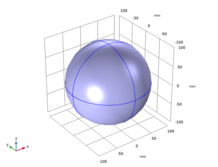
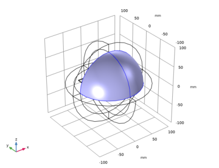
The radiation pattern of the uniform array factor configured to have the maximum radiation at 60 degrees from the x-axis by setting the value of alphax as in Table 2.
|

|
1
|
|
2
|
|
3
|
Click Add.
|
|
4
|
Click
|
|
5
|
|
6
|
Click
|
|
1
|
|
2
|
|
3
|
|
1
|
|
2
|
|
1
|
|
2
|
|
3
|
|
1
|
|
2
|
|
3
|
|
4
|
|
5
|
|
6
|
|
7
|
|
1
|
|
2
|
|
3
|
|
4
|
|
5
|
|
6
|
|
7
|
|
1
|
|
2
|
|
3
|
|
4
|
|
5
|
|
6
|
|
7
|
|
8
|
|
9
|
|
1
|
|
2
|
Select the object blk3 only.
|
|
3
|
|
4
|
|
5
|
|
1
|
|
2
|
Select the object blk2 only.
|
|
3
|
|
4
|
|
5
|
|
6
|
|
7
|
|
1
|
|
2
|
|
3
|
|
4
|
Click to expand the Layers section. In the table, enter the following settings:
|
|
5
|
|
6
|
|
1
|
|
2
|
|
3
|
|
4
|
|
5
|
|
6
|
|
1
|
|
2
|
|
1
|
|
2
|
|
1
|
|
2
|
|
1
|
|
2
|
|
3
|
|
4
|
|
5
|
Click OK.
|
|
1
|
|
2
|
|
3
|
|
4
|
|
5
|
Click OK.
|
|
1
|
|
2
|
|
3
|
|
4
|
|
5
|
In the Add dialog box, in the Selections to intersect list, choose PML, Exterior Boundaries and Air, Exterior Boundaries.
|
|
6
|
Click OK.
|
|
1
|
|
2
|
|
3
|
|
4
|
|
5
|
Click OK.
|
|
1
|
|
2
|
|
3
|
|
4
|
|
1
|
|
1
|
|
2
|
|
3
|
|
1
|
In the Model Builder window, under Component 1 (comp1) right-click Electromagnetic Waves, Frequency Domain (emw) and choose Perfect Electric Conductor.
|
|
1
|
|
2
|
|
3
|
|
4
|
|
1
|
|
2
|
|
3
|
In the tree, select Built-in>Air.
|
|
4
|
|
5
|
|
1
|
In the Model Builder window, under Component 1 (comp1) right-click Materials and choose Blank Material.
|
|
2
|
|
3
|
|
4
|
|
1
|
|
2
|
|
3
|
|
4
|
|
5
|
|
1
|
|
1
|
|
2
|
|
3
|
|
1
|
|
2
|
|
3
|
|
4
|
|
5
|
|
6
|
|
7
|
|
8
|
|
1
|
|
1
|
|
2
|
|
3
|
|
4
|
|
1
|
|
2
|
|
3
|
|
4
|
|
1
|
|
2
|
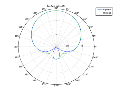
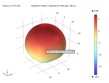
In the Settings window for Radiation Pattern, click Replace Expression in the upper-right corner of the Expression section. From the menu, choose Component 1 (comp1)>Electromagnetic Waves, Frequency Domain>Far field>emw.gaindBEfar - Far-field gain, dBi.
|
|
3
|
Locate the Evaluation section. Find the Reference direction subsection. In the x text field, type 0.
|
|
4
|
|
5
|
|
6
|
|
7
|
|
1
|
|
2
|
|
3
|
|
4
|
|
5
|
|
6
|
|
7
|
Click to expand the Coloring and Style section. Find the Line style subsection. From the Line list, choose Dashed.
|
|
8
|
Locate the Legends section. In the table, enter the following settings:
|
|
9
|
|
1
|
|
2
|
|
3
|
|
4
|
|
5
|
|
6
|
|
7
|
|
8
|
|
1
|
|
2
|
|
1
|
|
2
|
|
3
|
|
4
|
|
1
|
|
1
|
|
2
|
|
3
|
|
4
|
|
1
|
|
2
|
|
3
|
Find the Studies subsection. In the Select Study tree, select Preset Studies for Selected Physics Interfaces>Adaptive Frequency Sweep.
|
|
4
|
|
5
|
|
1
|
|
2
|
|
3
|
|
1
|
|
2
|
|
3
|
|
4
|
Locate the Values of Dependent Variables section. Find the Store fields in output subsection. From the Settings list, choose For selections.
|
|
5
|
|
6
|
|
7
|
Click OK.
|
|
8
|
|
1
|
|
2
|
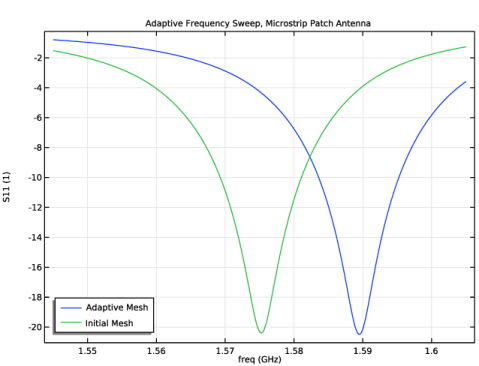
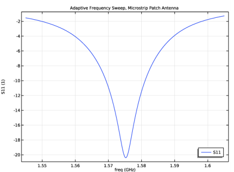
In the Settings window for 1D Plot Group, type S-parameter, Asymptotic Waveform Evaluation in the Label text field.
|
|
3
|
|
4
|
|
5
|
|
6
|
|
1
|
|
2
|
In the Settings window for Global, click Add Expression in the upper-right corner of the y-Axis Data section. From the menu, choose Component 1 (comp1)>Electromagnetic Waves, Frequency Domain>Ports>emw.S11dB - S11.
|
|
3
|
|
1
|
|
2
|
|
3
|
|
1
|
|
2
|
|
3
|
In the Expression text field, type emw.gaindBEfar+20*log10(emw.af3(8,8,1,0.48,0.48,0,0,0,0))+10*log10(1/64).
|
|
4
|
Select the Threshold check box.
|
|
6
|
Locate the Evaluation section. Find the Angles subsection. In the Number of elevation angles text field, type 180.
|
|
7
|
|
8
|
|
9
|
|
1
|
|
2
|
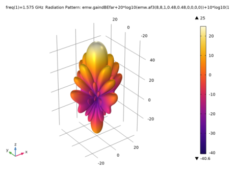
In the Settings window for Polar Plot Group, type 2D Far Field Gain (dB), Virtual Array in the Label text field.
|
|
3
|
|
4
|
|
5
|
|
6
|
|
7
|
|
8
|
|
1
|
In the 2D Far Field Gain (dB), Virtual Array toolbar, click
|
|
2
|
|
3
|
|
4
|
Locate the Evaluation section. Find the Angles subsection. In the Number of angles text field, type 360.
|
|
5
|
|
6
|
|
7
|
|
8
|
|
10
|
|
1
|
|
2
|
|
3
|
In the Expression text field, type 20*log10(emw.af3(8,8,1,0.48,0.48,0,-2*pi*0.48*cos(pi/3),0,0))+10*log10(1/64).
|
|
4
|
Locate the Legends section. In the table, enter the following settings:
|
|
5
|
|
1
|
|
2
|
|
3
|
In the Expression text field, type emw.gaindBEfar+20*log10(emw.af3(8,8,1,0.48,0.48,0,-2*pi*0.48*cos(pi/3),0,0))+10*log10(1/64).
|
|
4
|
Locate the Legends section. In the table, enter the following settings:
|
|
5
|
|
1
|
|
2
|
|
3
|
|
4
|
Locate the Layers section. In the table, enter the following settings:
|
|
5
|
|
6
|
|
1
|
|
2
|
|
3
|
Find the Studies subsection. In the Select Study tree, select Preset Studies for Selected Physics Interfaces>Frequency Domain, RF Adaptive Mesh.
|
|
4
|
|
5
|
|
1
|
|
2
|
Click
|
|
3
|
|
4
|
|
5
|
|
6
|
|
7
|
Click Replace.
|
|
8
|
|
9
|
|
10
|
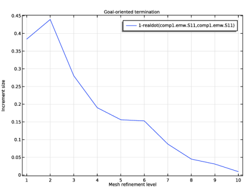
Clear the Generate default plots check box, as the default S-parameter and far-field plots are not of interest for the mesh adaptation study. However, in the following steps a field plot is built, so the mesh adaptation progress can be followed while solving.
|
|
1
|
|
2
|
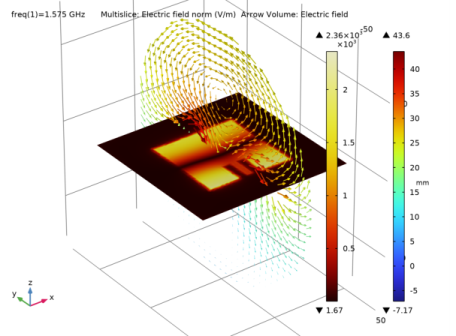
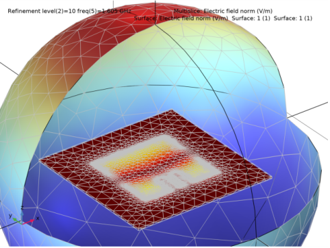
In the Settings window for 3D Plot Group, type Electric Field (emw), Mesh Adaptation in the Label text field.
|
|
3
|
Locate the Data section. From the Dataset list, choose Study 3/Adaptive Mesh Refinement Solutions 1 (sol4).
|
|
1
|
|
2
|
|
3
|
|
4
|
|
5
|
|
1
|
|
2
|
|
3
|
|
1
|
|
2
|
|
3
|
|
1
|
|
2
|
|
3
|
|
1
|
|
2
|
|
3
|
|
4
|
|
5
|
Click
|
|
1
|
In the Model Builder window, under Results>Electric Field (emw), Mesh Adaptation right-click Surface 1 and choose Duplicate, to add the first of two surface plots to visualize the mesh.
|
|
2
|
|
3
|
|
4
|
|
5
|
|
6
|
Select the Wireframe check box.
|
|
1
|
|
2
|
|
3
|
|
1
|
|
2
|
|
3
|
|
4
|
|
5
|
|
6
|
|
7
|
|
8
|
|
9
|
|
10
|
|
11
|
|
1
|
|
2
|
|
3
|
Find the Studies subsection. In the Select Study tree, select Preset Studies for Selected Physics Interfaces>Adaptive Frequency Sweep.
|
|
4
|
|
5
|
|
1
|
|
2
|
|
3
|
Clear the Generate default plots check box, as we again will not be saving the field in this study. Thereby, it doesn’t make sense generating the default field plots.
|
|
1
|
|
2
|
|
3
|
|
4
|
Locate the Values of Dependent Variables section. Find the Store fields in output subsection. From the Settings list, choose For selections.
|
|
5
|
|
6
|
|
7
|
Click OK.
|
|
8
|
|
1
|
|
2
|
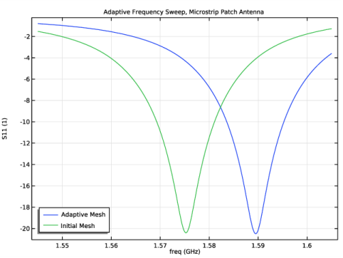
In the Settings window for 1D Plot Group, type S-parameter, Asymptotic Waveform Evaluation on Adaptive Mesh in the Label text field.
|
|
3
|
|
4
|
|
5
|
|
6
|
|
1
|
|
2
|
In the Settings window for Global, click Add Expression in the upper-right corner of the y-Axis Data section. From the menu, choose Component 1 (comp1)>Electromagnetic Waves, Frequency Domain>Ports>emw.S11dB - S11.
|
|
3
|
|
5
|
|
1
|
In the Model Builder window, right-click S-parameter, Asymptotic Waveform Evaluation on Adaptive Mesh and choose Paste Global.
|
|
2
|
|
3
|
|
4
|
Locate the Legends section. In the table, enter the following settings:
|
|
5
|