|
|
|

|
Scc11
|
||||
|
Scc12
|
||||
|
Scc21
|
||||
|
Scc22
|
||||
|
Scd11
|
||||
|
Scd12
|
||||
|
Scd21
|
||||
|
Scd22
|
||||
|
Sdc11
|
||||
|
Sdc12
|
||||
|
Sdc21
|
||||
|
Sdc22
|
||||
|
Sdd11
|
||||
|
Sdd12
|
||||
|
Sdd21
|
||||
|
Sdd22
|
|
1
|
|
2
|
|
3
|
Click Add.
|
|
4
|
Click
|
|
5
|
|
6
|
Click
|
|
1
|
|
2
|
|
1
|
|
2
|
|
3
|
|
1
|
|
2
|
|
3
|
|
4
|
|
5
|
|
6
|
|
7
|
|
1
|
|
2
|
|
3
|
|
1
|
|
2
|
|
3
|
|
4
|
|
5
|
|
1
|
|
2
|
|
3
|
|
4
|
|
5
|
|
1
|
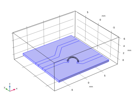
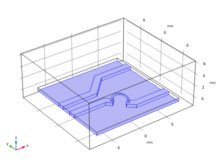
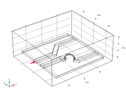
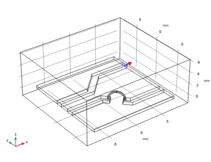
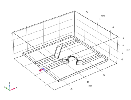
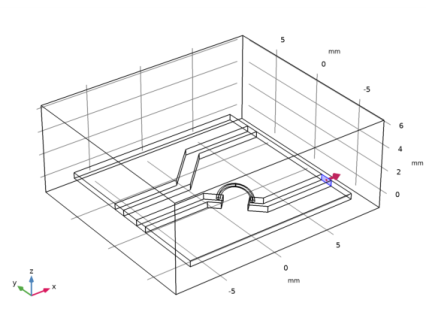
In the Model Builder window, under Component 1 (comp1)>Geometry 1>Work Plane 1 (wp1)>Plane Geometry right-click Rectangle 1 (r1) and choose Duplicate.
|
|
2
|
|
3
|
|
4
|
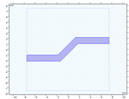
Locate the Position section. In the xw text field, type -sub_l/2+(sub_l/2-5/2/sqrt(2)+line_w/2/sqrt(2))/2.
|
|
5
|
|
1
|
|
2
|
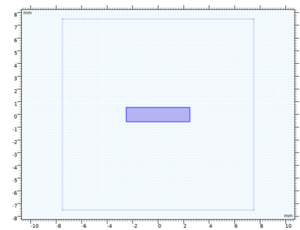
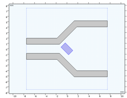
Select the object r2 only.
|
|
3
|
|
4
|
|
5
|
|
6
|
|
1
|
|
2
|
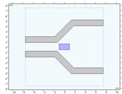
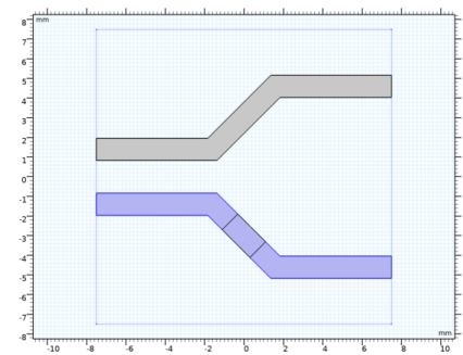
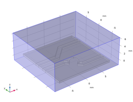
Click in the Graphics window and then press Ctrl+A to select all objects.
|
|
3
|
|
4
|
|
1
|
|
2
|
|
3
|
|
4
|
|
1
|
|
2
|
|
3
|
|
4
|
|
5
|
|
6
|
|
7
|
|
8
|
|
1
|
|
2
|
|
3
|
|
4
|
|
5
|
|
1
|
|
2
|
|
3
|
|
4
|
|
1
|
|
2
|
|
3
|
|
4
|
|
1
|
|
2
|
|
3
|
|
4
|
|
5
|
|
6
|
|
1
|
|
2
|
|
4
|
|
5
|
|
1
|
|
2
|
|
3
|
|
4
|
|
5
|
|
6
|
|
7
|
|
8
|
|
9
|
|
1
|
|
2
|
|
3
|
|
4
|
|
1
|
|
2
|
|
3
|
|
4
|
|
5
|
|
1
|
|
2
|
|
3
|
|
4
|
|
5
|
|
6
|
|
7
|
|
8
|
|
9
|
|
10
|
Click the
 |
|
1
|
|
2
|
|
3
|
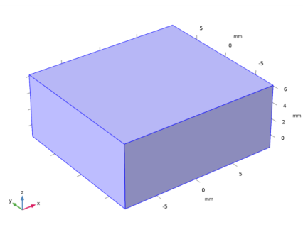
In the tree, select Built-in>Air.
|
|
4
|
|
5
|
|
1
|
In the Model Builder window, under Component 1 (comp1) right-click Materials and choose Blank Material.
|
|
3
|
|
1
|
In the Model Builder window, under Component 1 (comp1) right-click Electromagnetic Waves, Frequency Domain (emw) and choose Perfect Electric Conductor.
|
|
2
|
|
1
|
|
1
|
|
1
|
|
1
|
|
1
|
|
3
|
|
4
|
|
1
|
|
2
|
|
3
|
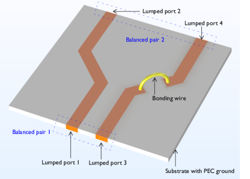
In the Port name for port B in balanced pair 1 text field, type 3. Balanced pair 1 includes port 1 and port 3.
|
|
4
|
In the Port name for port C in balanced pair 2 text field, type 2. Balanced pair 2 includes port 2 and port 4.
|
|
5
|
|
6
|
In the Settings window for Electromagnetic Waves, Frequency Domain, locate the Port Sweep Settings section.
|
|
7
|
|
8
|
Click Configure Sweep Settings. By clicking the Configure Sweep Settings button, all necessary port sweep settings such as sweep parameter and parametric study step will be automatically added. It is necessary to run the parametric sweep with port names to get a full S-parameter matrix and build the mixed mode S-parameters.
|
|
1
|
|
2
|
|
1
|
|
2
|
|
3
|
|
4
|
|
1
|
|
2
|
|
3
|
Click
|
|
4
|
|
5
|
|
6
|
|
7
|
Click Replace.
|
|
8
|
|
1
|
|
2
|
|
1
|
|
1
|
|
2
|
|
3
|
|
4
|
|
1
|
|
2
|
|
3
|
|
4
|
|
1
|
|
2
|
|
3
|
|
4
|
|
1
|
|
2
|
|
3
|
|
4
|
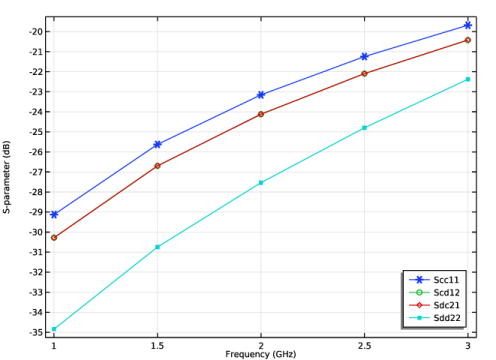
Click Add Expression in the upper-right corner of the y-Axis Data section. From the menu, choose Component 1 (comp1)>Electromagnetic Waves, Frequency Domain>Mixed-Mode S-Parameters 1>S-parameter, dB, common mode to common mode>emw.Scc11dB - Scc11.
|
|
5
|
Click Add Expression in the upper-right corner of the y-Axis Data section. From the menu, choose Component 1 (comp1)>Electromagnetic Waves, Frequency Domain>Mixed-Mode S-Parameters 1>S-parameter, dB, common mode to differential mode>emw.Scd12dB - Scd12.
|
|
6
|
Click Add Expression in the upper-right corner of the y-Axis Data section. From the menu, choose Component 1 (comp1)>Electromagnetic Waves, Frequency Domain>Mixed-Mode S-Parameters 1>S-parameter, dB, differential mode to common mode>emw.Sdc21dB - Sdc21.
|
|
7
|
Click Add Expression in the upper-right corner of the y-Axis Data section. From the menu, choose Component 1 (comp1)>Electromagnetic Waves, Frequency Domain>Mixed-Mode S-Parameters 1>S-parameter, dB, differential mode to differential mode>emw.Sdd22dB - Sdd22.
|
|
8
|
Click to expand the Coloring and Style section. Find the Line markers subsection. From the Marker list, choose Cycle.
|
|
9
|
|
10
|