|
|
|
|
1
|
|
2
|
|
3
|
Click Add.
|
|
4
|
Click
|
|
5
|
|
6
|
Click
|
|
1
|
|
2
|
|
3
|
|
1
|
|
2
|
|
3
|
Click
|
|
4
|
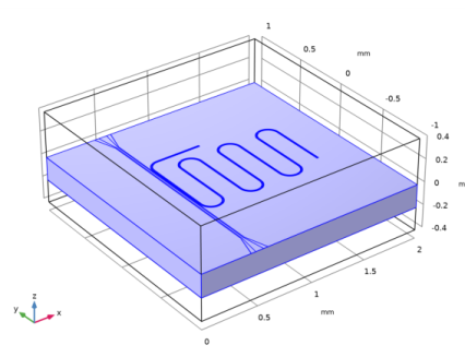
Browse to the model’s Application Libraries folder and double-click the file cpw_resonator.mphbin.
|
|
5
|
Click
|
|
6
|
|
1
|
In the Model Builder window, under Component 1 (comp1) right-click Electromagnetic Waves, Frequency Domain (emw) and choose Perfect Electric Conductor.
|
|
1
|
|
1
|
|
3
|
|
4
|
|
5
|
|
1
|
|
2
|
|
3
|
|
1
|
|
3
|
|
4
|
|
5
|
|
1
|
|
2
|
|
3
|
|
5
|
|
1
|
|
2
|
In the tree, select Built-in>Air.
|
|
3
|
|
4
|
In the tree, select Built-in>Silicon.
|
|
5
|
|
6
|
|
1
|
|
2
|
|
3
|
|
4
|
|
5
|
|
6
|
|
1
|
|
2
|
|
3
|
|
4
|
|
1
|
|
2
|
|
3
|
|
4
|
|
1
|
|
2
|
|
3
|
|
1
|
|
2
|
|
3
|
|
4
|
|
6
|
|
1
|
|
2
|
|
3
|
|
4
|
|
5
|
|
6
|
|
1
|
|
2
|
In the Settings window for Eigenfrequency, click to expand the Values of Dependent Variables section.
|
|
3
|
|
4
|
|
5
|
|
6
|
Click OK.
|
|
1
|
|
2
|
|
3
|
|
4
|
|
5
|
In the Model Builder window, expand the Study 1>Solver Configurations>Solution 1 (sol1)>Eigenvalue Solver 3 node.
|
|
6
|
Right-click Study 1>Solver Configurations>Solution 1 (sol1)>Eigenvalue Solver 3>Suggested Iterative Solver (emw) and choose Enable.
|
|
7
|
In the Model Builder window, expand the Study 1>Solver Configurations>Solution 1 (sol1)>Eigenvalue Solver 3>Suggested Iterative Solver (emw)>Multigrid 1 node.
|
|
8
|
Right-click Study 1>Solver Configurations>Solution 1 (sol1)>Eigenvalue Solver 3>Suggested Iterative Solver (emw)>Multigrid 1>Presmoother and choose Vanka.
|
|
9
|
|
10
|
|
11
|
|
12
|
|
13
|
Click OK.
|
|
14
|
|
15
|
|
16
|
|
17
|
In the Model Builder window, expand the Study 1>Solver Configurations>Solution 1 (sol1)>Eigenvalue Solver 3>Suggested Iterative Solver (emw)>Multigrid 1>Postsmoother node, then click SOR Vector 1.
|
|
18
|
|
19
|
|
20
|
|
21
|
|
1
|
|
2
|
|
3
|
|
4
|
|
5
|
|
1
|
|
2
|
|
3
|
|
4
|
|
5
|
|
6
|
|
1
|
In the Model Builder window, expand the Electric Mode Field, Port 2 (emw) node, then click Surface 1.
|
|
2
|
|
3
|
|
1
|
|
2
|
|
3
|
|
4
|
|
5
|
|
1
|
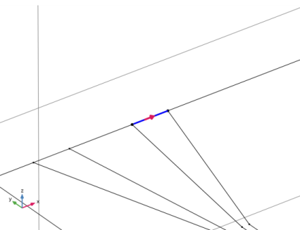
In the Model Builder window, under Study 1, Ctrl-click to select Step 1: Boundary Mode Analysis and Step 2: Boundary Mode Analysis 1.
|
|
2
|
Right-click and choose Copy.
|
|
1
|
|
2
|
|
3
|
|
1
|
|
2
|
|
3
|
|
4
|
|
1
|
|
2
|
|
3
|
|
1
|
|
2
|
In the Settings window for Adaptive Frequency Sweep, locate the Values of Dependent Variables section.
|
|
3
|
|
4
|
|
5
|
|
6
|
Click OK.
|
|
7
|
|
1
|
|
2
|
|
3
|
|
1
|
|
2
|
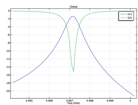
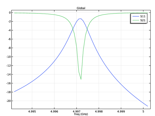
In the Settings window for Global, click Replace Expression in the upper-right corner of the y-Axis Data section. From the menu, choose Component 1 (comp1)>Electromagnetic Waves, Frequency Domain>Ports>S-parameter, dB>emw.S11dB - S11.
|
|
3
|
Click Add Expression in the upper-right corner of the y-Axis Data section. From the menu, choose Component 1 (comp1)>Electromagnetic Waves, Frequency Domain>Ports>S-parameter, dB>emw.S21dB - S21.
|
|
4
|