|
|
|
|
|
|||
|
|
(4)
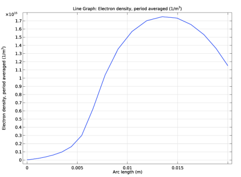
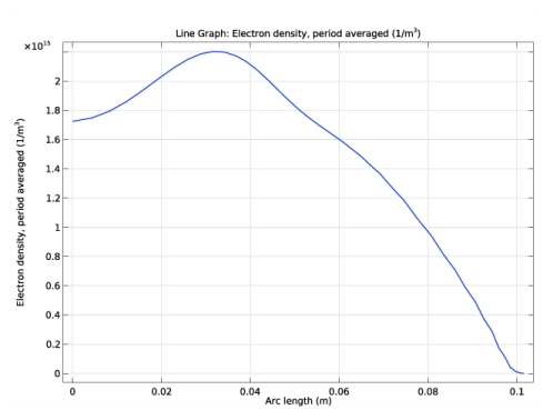
where the brackets represent the period averaged. To obtain electron temperatures similar to the ones in Ref. 1the average should be computed as
(5)
|
|
1
|
In the Model Wizard window, The Plasma, Time Periodic interface will be used to compute the periodic steady state solution for the GEC reference cell, using the Time Periodic study.
|
|
2
|
|
3
|
|
4
|
Click Add.
|
|
5
|
Click
|
|
6
|
|
7
|
Click
|
|
1
|
|
2
|
|
1
|
|
2
|
|
3
|
|
4
|
|
5
|
|
1
|
|
2
|
|
3
|
|
4
|
|
5
|
|
6
|
|
7
|
|
8
|
|
1
|
|
2
|
|
3
|
|
4
|
|
1
|
|
2
|
|
3
|
|
4
|
|
1
|
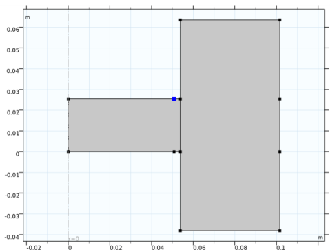
In the Model Builder window, under Component 1 (comp1)>Geometry 1 right-click Point 1 (pt1) and choose Duplicate.
|
|
2
|
|
3
|
|
4
|
|
1
|
In the Model Builder window, under Component 1 (comp1)>Geometry 1 right-click Point 2 (pt2) and choose Duplicate.
|
|
2
|
|
3
|
|
4
|
|
1
|
|
2
|
On the object pt2, select Point 1 only.
|
|
3
|
|
4
|
|
5
|
On the object pt1, select Point 1 only.
|
|
1
|
|
2
|
|
3
|
|
4
|
On the object fin, select Boundaries 4 and 9 only.
|
|
5
|
|
1
|
|
2
|
|
3
|
|
4
|
|
6
|
|
1
|
|
2
|
|
3
|
|
5
|
|
1
|
|
2
|
|
3
|
|
5
|
|
1
|
|
2
|
|
3
|
|
5
|
|
1
|
|
2
|
|
3
|
|
4
|
|
5
|
|
1
|
|
2
|
|
3
|
Click
|
|
4
|
Browse to the model’s Application Libraries folder and double-click the file Ar_xsecs_reduced.txt.
|
|
1
|
|
2
|
|
3
|
|
4
|
|
1
|
|
1
|
|
2
|
|
3
|
|
4
|
|
5
|
Click to collapse the Species Formula section. Click to expand the Mobility and Diffusivity Expressions section. From the Specification list, choose Specify mobility, compute diffusivity.
|
|
6
|
|
7
|
Click to expand the Mobility Specification section. From the Specify using list, choose Argon ion in argon.
|
|
1
|
|
2
|
|
3
|
|
4
|
|
5
|
|
1
|
|
2
|
|
3
|
|
4
|
|
5
|
Locate the Electron Density and Energy section. From the Electron transport properties list, choose Specify mobility only.
|
|
6
|
|
1
|
|
2
|
|
3
|
|
4
|
|
1
|
|
2
|
|
3
|
|
4
|
|
5
|
|
6
|
|
1
|
|
2
|
|
3
|
|
1
|
|
2
|
|
3
|
|
1
|
|
2
|
|
3
|
|
1
|
|
3
|
|
4
|
|
1
|
|
3
|
|
4
|
|
5
|
|
6
|
|
1
|
|
3
|
|
4
|
|
5
|
|
6
|
|
7
|
|
1
|
|
3
|
|
4
|
|
5
|
|
6
|
|
7
|
|
1
|
|
3
|
|
4
|
|
5
|
|
6
|
|
7
|
|
8
|
|
1
|
|
2
|
|
3
|
|
1
|
In the Model Builder window, expand the Time Periodic Study>Solver Configurations>Solution 1 (sol1) node.
|
|
2
|
In the Model Builder window, expand the Time Periodic Study>Solver Configurations>Solution 1 (sol1)>Stationary Solver 1 node, then click Fully Coupled 1.
|
|
3
|
|
4
|
Select the Plot check box.
|
|
5
|
|
1
|
|
2
|
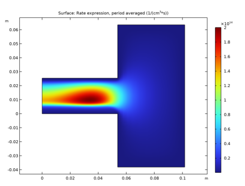
In the Settings window for 2D Plot Group, type Ionization Source, Period-Averaged in the Label text field.
|
|
1
|
|
2
|
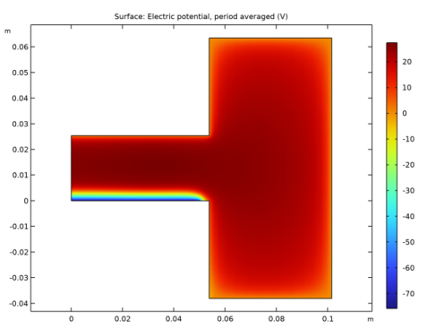
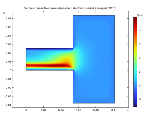
In the Settings window for Surface, click Replace Expression in the upper-right corner of the Expression section. From the menu, choose Component 1 (comp1)>Plasma, Time Periodic>Reaction rates>ptp.Re_av - Rate expression, period averaged - 1/(m³·s).
|
|
3
|
|
4
|
|
5
|
|
1
|
|
2
|
|
3
|
|
4
|
|
5
|
|
6
|
|
1
|
|
2
|
|
3
|
|
4
|
|
1
|
|
2
|
|
1
|
|
2
|
|
3
|
|
4
|
|
5
|
|
1
|
|
2
|
|
3
|
|
4
|
|
1
|
|
2
|
|
1
|
|
2
|
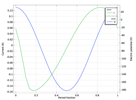
In the Settings window for Global Evaluation, click Replace Expression in the upper-right corner of the Expressions section. From the menu, choose Component 1 (comp1)>Plasma, Time Periodic>Metal Contact 1>ptp.mct1.Va_per - Voltage amplitude - V.
|
|
3
|
Click Add Expression in the upper-right corner of the Expressions section. From the menu, choose Component 1 (comp1)>Plasma, Time Periodic>Metal Contact 1>ptp.mct1.Vdcb_per - DC bias voltage - V.
|
|
4
|
Click
|
|
1
|
|
2
|
|
3
|
Find the Studies subsection. In the Select Study tree, select Preset Studies for Selected Physics Interfaces>Time Periodic to Time Dependent.
|
|
4
|
|
5
|
|
1
|
|
2
|
Click
|
|
3
|
|
4
|
|
5
|
|
6
|
Click Replace.
|
|
7
|
In the Settings window for Time Periodic to Time Dependent, click to expand the Values of Dependent Variables section.
|
|
8
|
Find the Values of variables not solved for subsection. From the Settings list, choose User controlled.
|
|
9
|
|
10
|
|
11
|
|
12
|
|
13
|
|
1
|
|
2
|
|
3
|