
|
|
|


|
1
|
|
2
|
In the Select Physics tree, select Structural Mechanics>Electromagnetics-Structure Interaction>Piezoresistivity>Piezoresistivity, Shell.
|
|
3
|
Click Add.
|
|
4
|
Click
|
|
5
|
|
6
|
Click
|
|
1
|
|
2
|
|
3
|
|
4
|
|
5
|
Browse to the model’s Application Libraries folder and double-click the file piezoresistive_pressure_sensor_shell_geom_sequence.mph.
|
|
6
|
|
1
|
|
2
|
|
3
|
|
1
|
|
2
|
|
3
|
|
1
|
|
2
|
|
3
|
|
4
|
|
5
|
|
6
|
|
7
|
|
8
|
|
1
|
|
2
|
|
3
|
|
4
|
|
5
|
|
6
|
Click OK.
|
|
1
|
|
2
|
|
3
|
|
4
|
|
5
|
|
6
|
|
7
|
Click OK.
|
|
1
|
|
2
|
|
3
|
|
4
|
|
5
|
|
6
|
Click OK.
|
|
7
|
|
8
|
|
1
|
|
2
|
|
3
|
|
4
|
|
5
|
|
6
|
Click OK.
|
|
7
|
|
8
|
|
9
|
|
10
|
Click OK.
|
|
11
|
|
1
|
|
2
|
|
3
|
|
1
|
|
2
|
|
3
|
|
4
|
|
5
|
|
6
|
|
7
|
|
1
|
|
2
|
|
1
|
|
2
|
|
3
|
|
1
|
|
2
|
|
3
|
|
1
|
|
2
|
|
3
|
|
4
|
|
1
|
In the Model Builder window, expand the Linear Elastic Material 1 node, then click Shell Local System 1.
|
|
2
|
|
3
|
|
1
|
|
2
|
|
3
|
|
1
|
|
2
|
|
3
|
|
1
|
|
2
|
|
3
|
|
4
|
|
5
|
|
1
|
In the Model Builder window, under Component 1 (comp1) click Electric Currents, Single Layer Shell (ecs).
|
|
2
|
In the Settings window for Electric Currents, Single Layer Shell, locate the Boundary Selection section.
|
|
3
|
|
4
|
|
5
|
|
6
|
|
7
|
In the Show More Options dialog box, in the tree, select the check box for the node Physics>Advanced Physics Options.
|
|
8
|
Click OK.
|
|
1
|
In the Model Builder window, under Component 1 (comp1)>Electric Currents, Single Layer Shell (ecs) click Current Conservation 1.
|
|
2
|
|
3
|
|
4
|
Locate the Coordinate System Selection section. From the Coordinate system list, choose Rotated System 2 (sys2).
|
|
1
|
|
2
|
|
3
|
|
4
|
|
5
|
Locate the Coordinate System Selection section. From the Coordinate system list, choose Rotated System 2 (sys2).
|
|
1
|
|
1
|
|
3
|
|
4
|
|
5
|
|
1
|
|
1
|
|
1
|
|
2
|
|
3
|
|
1
|
|
2
|
|
3
|
Click the Custom button.
|
|
4
|
|
5
|
|
1
|
|
2
|
|
3
|
|
4
|
|
5
|
|
6
|
|
1
|
|
2
|
|
3
|
|
4
|
|
1
|
|
2
|
|
3
|
|
5
|
|
1
|
|
2
|
|
3
|
|
4
|
|
1
|
|
2
|
|
1
|
|
2
|
|
3
|
|
4
|
|
1
|
|
2
|
|
3
|
|
1
|
|
2
|
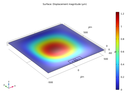
In the Settings window for Surface, click Replace Expression in the upper-right corner of the Expression section. From the menu, choose Component 1 (comp1)>Shell>Displacement>shell.disp - Displacement magnitude - m.
|
|
1
|
|
2
|
|
1
|
|
2
|
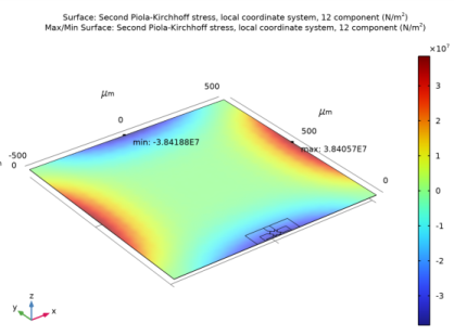
In the Settings window for 3D Plot Group, type In-Plane Shear Stress (Local Coordinates) in the Label text field.
|
|
3
|
|
1
|
|
2
|
In the Settings window for Surface, click Replace Expression in the upper-right corner of the Expression section. From the menu, choose Component 1 (comp1)>Shell>Stress>Second Piola-Kirchhoff stress, local coordinate system - N/m²>shell.Sl12 - Second Piola-Kirchhoff stress, local coordinate system, 12 component.
|
|
1
|
In the In-Plane Shear Stress (Local Coordinates) toolbar, click
|
|
2
|
In the Settings window for Max/Min Surface, click Replace Expression in the upper-right corner of the Expression section. From the menu, choose shell.Sl12 - Second Piola-Kirchhoff stress, local coordinate system, 12 component - N/m².
|
|
3
|
|
1
|
|
2
|
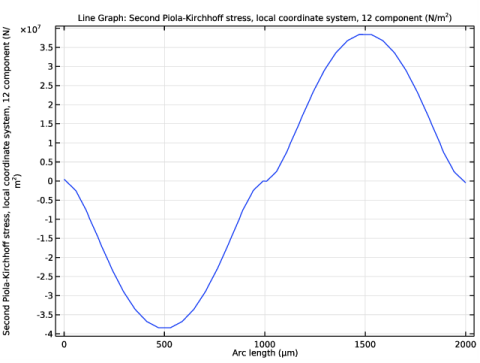
In the Settings window for 1D Plot Group, type In-Plane Shear Stress (Local Coordinate System) in the Label text field.
|
|
1
|
|
3
|
In the Settings window for Line Graph, click Replace Expression in the upper-right corner of the y-Axis Data section. From the menu, choose Component 1 (comp1)>Shell>Stress>Second Piola-Kirchhoff stress, local coordinate system - N/m²>shell.Sl12 - Second Piola-Kirchhoff stress, local coordinate system, 12 component.
|
|
4
|
|
1
|
|
2
|
|
3
|
|
4
|
|
5
|
|
1
|
|
2
|
|
3
|
|
1
|
|
2
|
|
3
|
|
4
|
|
5
|
|
6
|
|
1
|
|
2
|
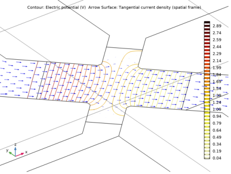
In the Settings window for Arrow Surface, click Replace Expression in the upper-right corner of the Expression section. From the menu, choose Component 1 (comp1)>Electric Currents, Single Layer Shell>Currents and charge>ecs.tJx,...,ecs.tJz - Tangential current density (spatial frame).
|
|
3
|
|
5
|
|
6
|
|
7
|
|
1
|
|
2
|
In the Settings window for Global Evaluation, click Replace Expression in the upper-right corner of the Expressions section. From the menu, choose Component 1 (comp1)>Electric Currents, Single Layer Shell>Terminals>ecs.I0_1 - Terminal current - A.
|
|
3
|
Click Add Expression in the upper-right corner of the Expressions section. From the menu, choose Component 1 (comp1)>Electric Currents, Single Layer Shell>Terminals>ecs.V0_2 - Terminal voltage - V.
|
|
4
|
Locate the Expressions section. In the table, enter the following settings:
|
|
5
|
Click
|
|
1
|
|
2
|
|
1
|
|
2
|
|
3
|
|
4
|
|
5
|
|
6
|
Click to expand the Layers section. In the table, enter the following settings:
|
|
7
|
|
8
|
|
9
|
|
1
|
|
2
|
|
3
|
|
4
|
|
1
|
|
2
|
|
3
|
|
4
|
|
5
|
|
6
|
|
7
|
Click to expand the Layers section. In the table, enter the following settings:
|
|
8
|
|
9
|
|
10
|
|
1
|
Right-click Component 1 (comp1)>Geometry 1>Work Plane 1 (wp1)>Plane Geometry>Rectangle 1 (r1) and choose Duplicate.
|
|
2
|
|
3
|
|
4
|
|
5
|
|
6
|
Locate the Layers section. In the table, enter the following settings:
|
|
1
|
|
2
|
|
3
|
|
4
|
|
5
|
|
6
|
|
1
|
|
2
|
|
3
|
|
4
|
|
5
|
|
6
|
|
1
|
|
2
|
|
3
|
|
4
|
|
5
|
|
6
|
|
1
|
|
2
|
|
3
|
|
4
|
|
5
|
|
6
|
|
1
|
|
2
|
|
3
|
|
4
|
|
5
|
|
6
|
|
1
|
|
2
|
|
3
|
|
4
|
|
1
|
In the Model Builder window, under Component 1 (comp1)>Geometry 1 right-click Work Plane 1 (wp1) and choose Virtual Operations>Form Composite Faces.
|
|
2
|
On the object fin, select Boundaries 19, 20, 26–35, and 38 only.
|
|
1
|
|
2
|
On the object cmf1, select Boundaries 11, 14–18, 25, 27, and 32–35 only.
|
|
1
|
|
2
|
On the object cmf2, select Edges 24 and 94 only.
|
|
3
|
|
4
|
|
1
|
|
2
|
On the object ige1, select Boundaries 7, 12, 15, 17, 21, and 24–26 only.
|
|
1
|
|
2
|
On the object cmf3, select Edges 4, 6, 8, 12, 84, and 87–89 only.
|
|
1
|
|
2
|
|
3
|
|
4
|
On the object ige2, select Boundary 9 only.
|
|
1
|
|
2
|
|
3
|
|
4
|
On the object ige2, select Boundaries 3, 5, 6, 8, 13–15, and 18 only.
|
|
1
|
|
2
|
|
3
|
|
4
|
|
5
|
|
6
|
|
7
|
|
8
|
|
1
|
|
2
|
|
3
|
|
4
|
|
5
|
|
6
|
Click OK.
|
|
1
|
|
2
|
|
3
|
|
4
|
|
5
|
|
6
|
Click OK.
|
|
1
|
|
2
|
|
3
|
|
4
|
Click
|
|
5
|
|
6
|
Click OK.
|
|
7
|
|
8
|
|
1
|
|
2
|
|
3
|
|
4
|
|
5
|
|
6
|
Click OK.
|
|
7
|
|
8
|
Click
|
|
9
|
|
10
|
Click OK.
|