PDF

Submarine Cable 3 — Bonding Capacitive
Introduction
Based on the results from the Capacitive Effects tutorial (the previous tutorial in this series), it is justified to neglect the capacitive coupling between the screens and consider one single isolated phase, together with its screen. As opposed to the Capacitive, Inductive, and Thermal Effects tutorials, this tutorial uses a 2D axisymmetric geometry representing the entire 10 kilometers of cable.
For several bonding types, the build-up of charging currents and the corresponding losses in the screen are analyzed (verification is included). The model validates the assumption that the high phase potential induces a uniform charging current — one that barely depends on the screen potential — and so justifies the approach chosen in the Capacitive and Inductive Effects tutorials (chapters 2, and 4).
Model Definition
The geometry is fairly simple; it contains only one phase. More precisely, it contains the cross-linked polyethylene (XLPE), the semi-conductive compound and the lead sheath surrounding the main conductor of that one phase; see Figure 1.
Figure 1: The cable's 2D axisymmetric geometry, including the semi-conductive compound (black), the cross-linked polyethylene (white) and the lead (red). The sections are used to reproduce the cross bonding configuration.
The use of a cylindrical coordinate system, together with the assumption that variations in the  direction may be neglected, turns the geometry into a strongly simplified 2D axisymmetric representation, that is; a couple of rectangles.
Theoretical Basis
When it comes to solving for the frequency domain current conservation problem, the methods used here are identical to the ones used in the Capacitive Effects tutorial. For more details on the involved theory, see the Capacitive Effects tutorial’s theory section.
Modeling Approach
The tutorial starts with the basics; by applying a phase voltage to the innermost boundary and connecting the screen to ground at one end only. This configuration is effectively the same as Single-Point Bonding. In a second step, the other end of the screen is connected to ground as well. The resulting configuration is effectively the same as Solid Bonding.
In a third step the geometry is modified, splitting the cable in three equal sections. Apart from the connections made by the screen, the individual sections are electrically insulated. Each section is given a separate phase voltage showing a 120° phase shift with respect to the other two. The screen is still grounded at both ends of the cable. The resulting configuration is effectively the same as Cross Bonding.
The results are verified using simple analytical models, based on the assumption that the charging current does not vary along the cable — see section On Charging Currents. Finally, you will be encouraged to try dissimilar section lengths, as this is something the model from the Capacitive Effects tutorial cannot do.
On Charging Currents
It is worth making a note on the unique way the current conservation laws manifest themselves in this case. As discussed in the Capacitive Effects tutorial, the charging current Ic in A/km is given by:
(1)
where C refers to the capacitance in μF/km, and V0 to the phase-to-ground voltage, of 127 kV. Strictly speaking, the value V0 refers to the potential difference between the phase and the screen, so Equation 1 should only hold when the screen potential is precisely 0 V. In practice, however, it also holds when the deviation from zero is insignificant compared to the large value of the phase voltage. This includes screen voltages up to several kilovolts.
Since the charging current barely depends on the screen voltage, it may be considered a constant. And as it is a constant in A/km, we may follow a reasoning where the currents are assumed to build up linearly along the length of the cable, reaching a maximum at the bonded ends and the intersections. This reasoning is used throughout this tutorial, for discussing bonding types, making predictions, and analyzing results.
Note: All analytical models used — and all predictions made — for the build up of charging currents in the screens, are based on the assumption that the charging current does not depend on the screen potential: Its phase may vary in time and space, but its magnitude will be constant. The numerical model is there to test this assumption.
On Bonding Types
Single-Point Bonding
In case of single-point bonding, each screen is electrically paired with the same phase across the entire length of the cable. Furthermore, it is bonded and connected to ground at one end only; see Figure 2. The phase potential will force a constant charging current that accumulates inside the screen. The screen currents build up linearly along the cable, reaching a maximum at the bonded end. At the floating end, the screen currents are zero and the screen potential reaches a maximum.
Figure 2: Schematic depiction of single-point bonding, where the screens (red, green, and blue) are bonded and grounded at one end only.
Because the screen potential at the floating end increases together with the cable’s length, this configuration is suitable for shorter stretches only. Because of the increased risk of corrosion, it is mainly used for terrestrial purposes (as opposed to submarine)1.
Solid Bonding
In case of solid bonding, each screen is still paired with a single phase, but this time it is bonded and connected to ground at both ends; see Figure 3. For the capacitive problem, this means the cable is cut in half. That is; a solid bonded cable can be considered as two single-point bonded cables of half the total length, who’s floating ends meet in the middle.
Now, the screen currents will build up in both directions, starting from zero at the center. At both ends they will reach a level that is one-half times the maximum screen current found for the single-point bonding configuration. The maximum screen potential will occur in the middle. Compared to the maximum screen potential from the single-point bonding configuration, it will be four times as small2.
Figure 3: Schematic depiction of solid bonding, where the screens (red, green, and blue) are bonded and grounded at both ends.
Cross Bonding
Cross bonding shows the most sophisticated configuration — and conceptually, the most elegant one. In case of cross bonding, the total length of cable is split in three sections of equal length. From an electrical point of view, the screen is paired with a different phase for each section; see Figure 4.
As the charging currents for the three sections show a 120° phase shift, it is not the norm of the screen current that will change linearly along the cable (as was the case for the other two bonding types). Instead, it is the complex current itself, that develops linearly along the cable sections. It interpolates between the three points where the current reaches a maximum; intersection 1, intersection 2, and the combination of the two bonding points.
Since the currents at these three locations are 120° out of phase, the three points of maximum current form an equilateral triangle on the complex plane, centered around zero. Each side of the triangle represents the current difference3 across one section, and has a length equal to one-third times the maximum screen current found for the single-point bonding configuration.
Figure 4: Schematic depiction of cross bonding, where the screens (red, green, and blue) are split in three cross-bonded sections of equal length.
The intersections increase the complexity of the cable system, and consequently, the risk of failure (due to leakage, corrosion and such). Therefore, like for single-point bonding, this configuration is not preferred for submarine cable systems4.
On Scaled Systems
The geometry is assumed to be 10 km long in the cable’s axial direction. In the radial direction, it contains features of about 1 mm thick. This extreme aspect ratio leads to challenges for the geometry sequence, the physics, the mesh and the plots.
In order to avoid this situation, a scaled coordinate system is used. In the axial direction the coordinates are scaled by a factor of 105. This allows for having a 10 cm long geometry, that is perceived by the physics as 10 km: The stretched space leads to much lower values for the spatial derivative in , so the electric field and the current density in the axial direction will be 105 times lower then what you would get for the unscaled 10 cm long model.
Since in-between the electric field E and the current density J there is still the factor of σ, from the current’s viewpoint, the scaled system is equivalent to an anisotropic conductor. That is, the two effects are interchangeable: An unscaled system with an anisotropic conductivity may produce the same currents.
Conversely, an anisotropic conductivity can be used to partially compensate for the scaling. This is done in order to keep the model numerically stable. The numerical stability issues encountered here, are similar to those seen in the Capacitive Effects tutorial.
Results and Discussion
When using Single-Point Bonding, the current builds up to 55 A at the bonded end for each screen individually. The maximum screen potential becomes 83 V, and the total losses per screen evaluate to 1.5 kW.
When using Solid Bonding the current builds up to 28 A, the maximum screen potential becomes 21 V, and the total losses per screen evaluate to 0.38 kW.
Finally, when Cross Bonding is applied, the maximum current is 10.7 A. This current occurs at the two intersections and the bonded ends. The currents at these locations show a 120° phase shift with respect to one another. The maximum screen potential occurs half-way the cable. It has a norm of 6.9 V. The losses have been reduced to as little as 85 W.
Apart from a minor deviation caused by the anisotropic conductivity (see section On Scaled Systems) all results agree perfectly well with the analytic approximation, in which a linear accumulation of charging currents is assumed, see section On Charging Currents.
This validates the assumptions made in the Capacitive Effects tutorial. Perhaps more importantly, it shows that the capacitive problem and the inductive problem can be considered separate issues:
Therefore, this result validates the use of separate models for investigating inductive and capacitive effects, as is done in this tutorial series.
Reference
1. Video file submarine_cable_z_animation_03_cross_bonding,
available for download at https://www.comsol.com/model/43431.
Application Library path: ACDC_Module/Tutorials,_Cables/submarine_cable_03_bonding_capacitive
Modeling Instructions
From the File menu, choose New.
New
In the New window, click  Model Wizard.
Model Wizard
1
In the Model Wizard window, click  2D Axisymmetric.
2
In the Select Physics tree, select AC/DC>Electric Fields and Currents>Electric Currents (ec).
3
4
Click  Study.
5
In the Select Study tree, select General Studies>Frequency Domain.
6
Global Definitions
This model uses a subset of the parameters already defined for the other tutorials. In order to gain access to them, you can load them all.
Geometric Parameters 1
1
In the Model Builder window, under Global Definitions click Parameters 1.
2
In the Settings window for Parameters, type Geometric Parameters 1 in the Label text field.
3
Locate the Parameters section. Click  Load from File.
4
Geometric Parameters 2
1
In the Home toolbar, click  Parameters and choose Add>Parameters.
2
In the Settings window for Parameters, type Geometric Parameters 2 in the Label text field.
3
Locate the Parameters section. Click  Load from File.
4
Electromagnetic Parameters
1
In the Home toolbar, click  Parameters and choose Add>Parameters.
2
In the Settings window for Parameters, type Electromagnetic Parameters in the Label text field.
3
Locate the Parameters section. Click  Load from File.
4
Definitions
The cable is 10 km long and contains features of about 1 mm thick. This extreme aspect ratio leads to challenges for the geometry sequence, the physics, the mesh and the plots. In order to avoid this situation, the coordinate system is scaled in the axial direction by a factor of Scab; 105. This will make the cable seem 10 km, even though the actual geometry is only 10 cm long (see section On Scaled Systems).
Scaling System 2 (sys2)
1
In the Definitions toolbar, click  Coordinate Systems and choose Scaling System.
2
In the Settings window for Scaling System, locate the Domain Selection section.
3
From the Selection list, choose All domains.
4
Locate the Settings section. Find the Coordinate mapping subsection. In the table, enter the following settings:
Geometry 1
The geometry contains only one phase. More precisely, it contains the insulators and the screen surrounding the main conductor of that one phase. In the 2D axisymmetric representation, this translates to a couple of rectangles. The first rectangle that is added will seem superfluous at first. It will be used to split the cable into sections later.
Rectangle 1 (r1)
1
In the Geometry toolbar, click  Rectangle.
2
In the Settings window for Rectangle, locate the Size and Shape section.
3
In the Width text field, type Dins/2+Tpbs-Dcon/2.
4
In the Height text field, type Lcab/Scab.
(Note that the division by Scab compensates for the effects of the scaling system).
5
Locate the Position section. In the r text field, type Dcon/2.
Rectangle 2 (r2)
1
Right-click Rectangle 1 (r1) and choose Duplicate.
2
In the Settings window for Rectangle, click to expand the Layers section.
3
4
Select the Layers to the left check box.
5
Clear the Layers on bottom check box.
Form Union (fin)
1
In the Geometry toolbar, click  Build All.
2
Click the  Zoom Extents button in the Graphics toolbar.
Definitions
The materials are roughly the same as those used in the Capacitive Effects tutorial. To start with, you can modify the View to show the material colors. Then, the materials will be added, they will be given an appropriate label, a selection and an appearance.
View 1
1
In the Model Builder window, under Component 1 (comp1)>Definitions click View 1.
2
In the Settings window for View, locate the Colors section.
3
Select the Show material color and texture check box.
Materials
Semi-conductive compound
1
In the Model Builder window, under Component 1 (comp1) right-click Materials and choose Blank Material.
2
In the Settings window for Material, type Semi-conductive compound in the Label text field.
3
Click the  Zoom to Selection button in the Graphics toolbar.
A good approach is to assign the first material to all domains by default. Subsequently, you can override it locally, using additional materials. This ensures every domain has access to material properties.
4
Click to expand the Appearance section. From the Color list, choose Black.
Cross-linked polyethylene (XLPE)
1
Right-click Materials and choose Blank Material.
2
In the Settings window for Material, type Cross-linked polyethylene (XLPE) in the Label text field.
3
4
Click to expand the Appearance section.  
Notice that “white plastic” is the default setting. Leave it unchanged.
Lead
1
Right-click Materials and choose Blank Material.
2
In the Settings window for Material, type Lead in the Label text field.
3
4
Click to expand the Appearance section. From the Material type list, choose Lead.
Materials
Now, you will see that COMSOL starts detecting missing material properties. The properties that should be added are listed in the following table. Please check all of them for the correct value, even the ones that are already filled in. Note that for cases like this, a convenient option is to copy-paste the values directly from this *.pdf file to COMSOL.
1
In the Model Builder window, under Component 1 (comp1)>Materials, add the following material properties:
Modeling Instructions — Single-Point Bonding
In case of single-point bonding, the screen is electrically paired with the same phase across the entire length of the cable. Furthermore, it is bonded and grounded at one end only, see section Single-Point Bonding.
From the Capacitive Effects tutorial, we know that about 5.5 A will leak from the central conductor each kilometer (as given by Icpha). Based on the assumption that the potential of the central conductor and the screen remains more or less constant along the cable, we expect that the charging currents in the screen will build up linearly (see section On Charging Currents). At the ground point, a total of Lcab*Icpha will leave the cable. This evaluates to about 55 A.
Since the current builds up linearly, the average current will be 1/2*Lcab*Icpha, that is; (55 A)/2. Consequently, the screen potential at the free end of the cable will be 1/2*Lcab*Icpha*Lcab*Rpbs, and the total RMS losses per phase, |I|2R/2, will be 1/6*(Lcab*Icpha)^2*Lcab*Rpbs. This evaluates to 83 V and 1.5 kW respectively (where the variable names refer to the parameters used throughout this tutorial series).
The expected 83 V raise seems to contradict the assumption of the screen potential being constant along the cable. Compared to the 127 kV on the main conductor however, it will be negligible. Let us see if we can reproduce these results. Start by introducing an anisotropic conductivity for the lead.
Electric Currents (ec)
Current Conservation 2
1
In the Model Builder window, under Component 1 (comp1) right-click Electric Currents (ec) and choose Current Conservation.
2
3
In the Settings window for Current Conservation, locate the Constitutive Relation Jc-E section.
4
From the σ list, choose User defined. From the list, choose Diagonal.
5
In the σ table, enter the following settings:
In order to get the model numerically stable, you have now scaled the r-component of the conductivity. From an electrical viewpoint, the extreme aspect ratio caused by the coordinate transformation has been compensated for (see section On Scaled Systems).
This compensation will not influence the results significantly though, as even with this large scale factor, the lead is still by far the best conductor in the radial direction: The insulators will determine the current. This reasoning is similar to the one applied in the Capacitive Effects tutorial, when setting the conductors to 5 S/m.
In the z direction however, the materials are placed in parallel (as opposed to series), and the lead will dominate. In this direction it is important to use a realistic value for the lead conductivity. The ϕ direction is of limited significance. Because of symmetry reasons, there will be no current flowing in that direction (the model solves for in-plane currents only).
Next, add a ground point and an electric potential for the central conductor.
Ground 1
1
In the Physics toolbar, click  Boundaries and choose Ground.
2
Select Boundary 11 only, (on the bottom-right).
Phase 1
1
In the Physics toolbar, click  Boundaries and choose Electric Potential.
2
In the Settings window for Electric Potential, type Phase 1 in the Label text field.
3
4
Locate the Electric Potential section. In the V0 text field, type (V0-(I0*Rcon*sys2.z)).
Here, for the sake of completeness we have included an approximation of the potential drop caused by the currents in the main conductor, using the z-coordinate from the scaling system and the phase DC resistance. At the end of the cable, the potential drop should be about I0*Rcon*Lcab, that is; 311 V. Proceed by computing the solution.
Study 1
Step 1: Frequency Domain
1
In the Model Builder window, under Study 1 click Step 1: Frequency Domain.
2
In the Settings window for Frequency Domain, locate the Study Settings section.
3
In the Frequencies text field, type f0.
4
In the Home toolbar, click  Compute.
Results
Electric Potential (ec)
The default plot is not very informative in this case. Let us make some 1D plots to investigate the currents and voltages in the screen.
Electric Potential Norm, 1D (ec)
1
In the Home toolbar, click  Add Plot Group and choose 1D Plot Group.
2
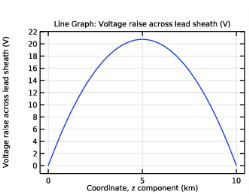
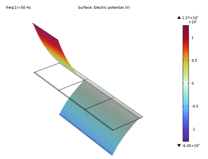
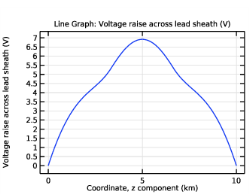
In the Settings window for 1D Plot Group, type Electric Potential Norm, 1D (ec) in the Label text field.
Line Graph 1
1
Right-click Electric Potential Norm, 1D (ec) and choose Line Graph.
2
3
In the Settings window for Line Graph, locate the y-Axis Data section.
4
In the Expression text field, type abs(V).
5
Select the Description check box.
6
In the associated text field, type Voltage raise across lead sheath.
7
Locate the x-Axis Data section. From the Parameter list, choose Expression.
8
In the Expression text field, type sys2.z.
9
From the Unit list, choose km.
10
In the Electric Potential Norm, 1D (ec) toolbar, click  Plot.
The plot should look like half a parabola (upside down) and reach 83 V, as predicted. This suggests the assumption of the linear increase of screen currents along the cable is justified.
Let us check those currents, and the corresponding losses.
Electric Current Norm, 1D (ec)
1
In the Home toolbar, click  Add Plot Group and choose 1D Plot Group.
2
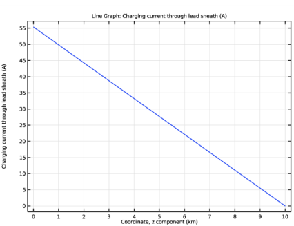
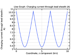
In the Settings window for 1D Plot Group, type Electric Current Norm, 1D (ec) in the Label text field.
Line Graph 1
1
Right-click Electric Current Norm, 1D (ec) and choose Line Graph.
2
3
In the Settings window for Line Graph, locate the y-Axis Data section.
4
In the Expression text field, type ec.normJ*Apbs.
5
Select the Description check box.
6
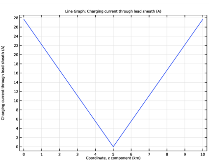
In the associated text field, type Charging current through lead sheath.
7
Locate the x-Axis Data section. From the Parameter list, choose Expression.
8
In the Expression text field, type sys2.z.
9
From the Unit list, choose km.
10
In the Electric Current Norm, 1D (ec) toolbar, click  Plot.
For this plot, you have multiplied the current density norm ec.normJ by the cross section of the lead sheath to get the total current per phase, along the cable. The current near the ground point should be 55 A.
Resistive Losses
1
In the Results toolbar, click  More Derived Values and choose Integration>Surface Integration.
2
In the Settings window for Surface Integration, type Resistive Losses in the Label text field.
3
Locate the Selection section. From the Selection list, choose All domains.
4
Locate the Expressions section. In the table, enter the following settings:
5
Click  Evaluate.
Table
1
Go to the Table window.
For the losses, the quantity ec.Qh has been multiplied with Scab, to compensate for the scaling (as the integration operator is unaware of the scale factor). The total losses per phase should be about 1.5 kW (the value deviates from the analytical result by 0.5% or so, due to scaling the r-component of the lead conductivity).
Notice that all domains have been selected here, while the analytical prediction only considers the screen. The fact that the results agree, suggests no significant losses occur in the insulators. This is according to our expectations, feel free to check this.
Now, one could argue single-point bonding is almost too simple to build a model for. Indeed, you can consider this a verification: We know now our general reasoning is sound and COMSOL is able to reproduce it within 1%, at least. The next bonding types will be a bit less obvious.
Modeling Instructions — Solid Bonding
In case of solid bonding, the screen is bonded and grounded at both ends, see section Solid Bonding. Since the charging current now only has half a cable to accumulate, the current near the ground points will be 1/2*Lcab*Icpha, or 28 A. For the voltage and the losses a similar reasoning holds. We get 1/8*Lcab*Icpha*Lcab*Rpbs, and 1/24*(Lcab*Icpha)^2*Lcab*Rpbs, which evaluates to 21 V and 0.38 kW respectively.
Proceed by reproducing this arrangement.
Electric Currents (ec)
Ground 1
1
In the Model Builder window, under Component 1 (comp1)>Electric Currents (ec) click Ground 1.
2
Study 1
In the Home toolbar, click  Compute.
Results
Electric Potential Norm, 1D (ec)
1
In the Model Builder window, under Results click Electric Potential Norm, 1D (ec).
2
In the Electric Potential Norm, 1D (ec) toolbar, click  Plot.
Electric Current Norm, 1D (ec)
1
In the Model Builder window, click Electric Current Norm, 1D (ec).
2
In the Electric Current Norm, 1D (ec) toolbar, click  Plot.
Resistive Losses
1
In the Model Builder window, under Results>Derived Values click Resistive Losses.
2
In the Settings window for Surface Integration, click  Evaluate.
Table
1
Go to the Table window.
The maximum potential is about 21 V, the maximum current is 28 A, and the total losses are about 0.38 kW per screen (as analytically predicted).
Modeling Instructions — Cross Bonding
In case of cross bonding, the total length of cable is split in three sections of equal length. From an electrical point of view, the screen is paired with a different phase for each section. Consequently, for a well balanced cable, the total net current that enters the screen is zero (see section Cross Bonding).
Let us proceed by reproducing this arrangement. Start by splitting the cable in three parts.
Geometry 1
Rectangle 1 (r1)
1
In the Model Builder window, under Component 1 (comp1)>Geometry 1 click Rectangle 1 (r1).
2
In the Settings window for Rectangle, locate the Layers section.
3
Form Union (fin)
1
In the Home toolbar, click  Build All.
2
Click the  Zoom Extents button in the Graphics toolbar.
Now that the cable is divided in three equal sections, apply a different phase potential to each of them.
Electric Currents (ec)
Phase 1
1
In the Model Builder window, under Component 1 (comp1)>Electric Currents (ec) click Phase 1.
2
Phase 2
1
In the Physics toolbar, click  Boundaries and choose Electric Potential.
2
In the Settings window for Electric Potential, type Phase 2 in the Label text field.
3
4
Locate the Electric Potential section. In the V0 text field, type (V0-(I0*Rcon*sys2.z))*exp(-120[deg]*j).
Note that for longer expressions like this one, the easiest way to go, is to copy-paste them directly from this *.pdf file to COMSOL.
Phase 3
1
In the Physics toolbar, click  Boundaries and choose Electric Potential.
2
In the Settings window for Electric Potential, type Phase 3 in the Label text field.
3
4
Locate the Electric Potential section. In the V0 text field, type (V0-(I0*Rcon*sys2.z))*exp(+120[deg]*j).
Since we are in the frequency domain here, expressions like exp(-120[deg]*j) or exp(-j*2*pi/3) may be used to set a 120° phase shift between the AC voltages on the three main conductors.
Lastly, as the model now represents three separate phases (only the screen is electrically continuous), you will need to add some insulation in-between.
Electric Insulation 2
1
In the Physics toolbar, click  Boundaries and choose Electric Insulation.
2
In the Settings window for Electric Insulation, locate the Boundary Selection section.
3
Click  Paste Selection.
4
In the Paste Selection dialog box, type 4, 6, 11, 13, 18, 20 in the Selection text field.
5
Study 1
In the Home toolbar, click  Compute.
Results
Electric Potential (ec)
These results are phase dependent. Therefore, the default plot Electric Potential, may be a bit deceiving. Create an animation to see what is going on.
Streamline 1
1
In the Model Builder window, expand the Electric Potential (ec) node.
2
Right-click Streamline 1 and choose Disable.
Surface 1
1
In the Model Builder window, click Surface 1.
2
In the Settings window for Surface, locate the Coloring and Style section.
3
From the Scale list, choose Linear symmetric.
Height Expression 1
1
Right-click Surface 1 and choose Height Expression.
2
In the Electric Potential (ec) toolbar, click  Plot.
3
Click the  Go to Default View button in the Graphics toolbar.
Animation 1
1
In the Results toolbar, click  Animation and choose Player.
2
In the Settings window for Animation, locate the Animation Editing section.
3
From the Sequence type list, choose Dynamic data extension.
4
Locate the Frames section. In the Number of frames text field, type 60.
5
Locate the Playing section. From the Repeat list, choose Forever.
6
Click the  Play button in the Graphics toolbar (see the animation from ref. [1]).
So the different phases are exchanging currents. Now, the currents will not have to build-up all the way to the ground point. Instead, they are compensated for within the cable. As a result, the average current, the potential and the losses in the screen are reduced significantly. Let us investigate to what extent this is the case.
7
Click the Stop button in the Graphics toolbar.
Electric Potential Norm, 1D (ec)
1
In the Model Builder window, under Results click Electric Potential Norm, 1D (ec).
2
In the Electric Potential Norm, 1D (ec) toolbar, click  Plot.
Electric Current Norm, 1D (ec)
1
In the Model Builder window, click Electric Current Norm, 1D (ec).
2
In the Electric Current Norm, 1D (ec) toolbar, click  Plot.
Resistive Losses
1
In the Model Builder window, under Results>Derived Values click Resistive Losses.
2
In the Settings window for Surface Integration, click  Evaluate.
Table
1
Go to the Table window.
The maximum current is 10.7 A. This current occurs at the two intersections and the bonded ends. The maximum potential is about 6.9 V, and the total losses are about 85 W per screen.
What these results tell us is that from a loss point of view, cross bonding is not a bad idea. Secondly, we see that there is little or no effect of the bonding types on the charging currents: Since the 127 kV that is put on the central conductors is huge compared to any of the other potentials we have seen coming by (including the ones from the Bonding Inductive tutorial), the charging current will always be about 5.5 A/km. In other words, the reasoning proposed in section On Charging Currents, is valid.
Furthermore, we see that the resulting current densities are small compared to those in the Inductive Effects tutorial. As a result, there is only a weak coupling between the inductive and capacitive part of the device, justifying the approach chosen for these tutorials. Finally, one thing this model can do that most of the others cannot, is showing the effect of having sections of dissimilar length. Please feel free to change Lsec1 and Lsec3be careful not to put them to zero though, as it changes the number of sections.
You have now completed this tutorial, subsequent tutorials will refer to the resulting file as submarine_cable_03_bonding_capacitive.mph. The next tutorial in this series will include a detailed inductive analysis.
1
From the File menu, choose Save As.
2
Browse to a suitable folder and type the filename submarine_cable_03_bonding_capacitive.mph.
 

1
Treatment of the single-point bonding configuration within the context of this submarine cable tutorial series should therefore be seen as a demonstration of a concept, rather than a demonstration of a real-world application. Including these bonding types extends this tutorial series to a point where it is useful for demonstrating terrestrial applications as well.

2
As the voltage equals the current times the resistance, and both the average accumulated current, as well as the total resistance, are directly (linearly) proportional to the length of the cable.

3
This is analogous to a potential difference for voltage-driven problems.

4
Treatment of the cross bonding configuration within the context of this submarine cable tutorial series should therefore be seen as a demonstration of a concept, rather than a demonstration of a real-world application.