You are viewing the documentation for an older COMSOL version. The latest version is available here.
PDF

Electric Shielding Comparison
Introduction
The electric shielding boundary condition is meant to approximate a thin layer of highly conductive material that provides an additional current path tangential to a boundary. This example compares the electric shielding boundary condition to a full-fidelity model and discusses the range of applicability of this boundary condition.
Figure 1: A square 2D domain of conductive material, with a circular inclusion. The wall of the inclusion are made of a material with higher conductivity.
Model Definition
The situation being modeled is shown in Figure 1. A 1 m square two-dimensional domain of conductive material has a DC voltage difference applied to it. Within the square domain, there is a circular inclusion of radius 0.25 m. The 0.01 m thick walls of this inclusion are modeled two ways, first using a full fidelity model that includes the thickness of the walls, and also using the electric shielding boundary condition. The inside of the inclusion has the same properties as the bulk.
The location of the electric shielding condition is at the centerline, midway between the inner and outer radii of the full fidelity model. Note that, when using the electric shielding condition, the total volume of the surrounding material is slightly larger, since the thickness of the wall is not being explicitly modeled. The conductivity of the wall of the inclusion is varied.
Results and Discussion
The voltage distribution and the electric field strength is plotted in Figure 2 for the case where the electric conductivity is one thousand times greater in the wall of the inclusion than in the bulk. This represents a thin walled object that allows significant current flow along its surface, that is, it shields whatever is inside the inclusion from the electric fields and current flow. The current can be observed to flow toward the inclusion, and then along the surface. The solutions for the full fidelity and electric shielding model agree well for the cases where the conductivity is greater than the surrounding medium.
Figure 2: A surface plot of the electric field norm, together with isolines of the electric potential and an arrow plot indicating the electric field direction, for the case of a thin layer of material that has a high conductivity. The full fidelity (left) and electric shielding (right) solutions are almost identical.
Figure 3 shows the case where the electric conductivity in the wall of the inclusion is only ten times greater than the surroundings. The electric shielding condition still agrees well with the full fidelity model.
Figure 3: A surface plot of the electric field norm, together with isolines of the electric potential and an arrow plot indicating the electric field direction, for the case of a thin layer of material that has conductivity ten times greater than the surrounding material.
Figure 4 shows the case where the electric conductivity in the wall of the inclusion is ten times less than the surroundings. The electric shielding condition no longer agrees with the full fidelity model. Although an additional conduction path has been added tangential to the boundary, the magnitude of this conduction path is less than in the surrounding material, thus it does not noticeably alter the current flow. The electric shielding boundary condition also does not impede the current flow normal to the boundary, which is the case, as can be seen in the full fidelity model. The Contact Impedance boundary condition would be more appropriate for this case.
The electric shielding boundary condition can be used in cases where the thickness of the boundary being approximated is much smaller than the characteristic size of the model domain, and when the conductivity of the layer is greater than the surrounding medium. When this boundary condition can be used, the resulting mesh size is much smaller, saving solution time and memory.
Figure 4: For the case of a thin layer of material that has conductivity ten times less than the surrounding material. The solutions do not agree for this case.
Application Library path: ACDC_Module/Resistive_Devices/electric_shielding_comparison
Modeling Instructions
From the File menu, choose New.
New
In the New window, click  Model Wizard.
Model Wizard
1
In the Model Wizard window, click  2D.
2
In the Select Physics tree, select AC/DC>Electric Fields and Currents>Electric Currents (ec).
3
Click Add.
4
Click  Study.
5
In the Select Study tree, select General Studies>Stationary.
6
Global Definitions
Parameters 1
1
In the Model Builder window, under Global Definitions click Parameters 1.
2
In the Settings window for Parameters, locate the Parameters section.
3
Geometry 1
Square 1 (sq1)
1
In the Geometry toolbar, click  Square.
2
In the Settings window for Square, locate the Position section.
3
In the x text field, type 0.05.
Square 2 (sq2)
1
In the Geometry toolbar, click  Square.
2
In the Settings window for Square, locate the Position section.
3
In the x text field, type -1.05.
Circle 1 (c1)
1
In the Geometry toolbar, click  Circle.
2
In the Settings window for Circle, locate the Size and Shape section.
3
In the Radius text field, type 0.245.
4
Locate the Position section. In the x text field, type 0.55.
5
In the y text field, type 0.5.
Circle 2 (c2)
1
In the Geometry toolbar, click  Circle.
2
In the Settings window for Circle, locate the Size and Shape section.
3
In the Radius text field, type 0.25.
4
Locate the Position section. In the x text field, type -0.55.
5
In the y text field, type 0.5.
6
Click to expand the Layers section. In the table, enter the following settings:
Form Union (fin)
1
In the Geometry toolbar, click  Build All.
2
Click the  Zoom Extents button in the Graphics toolbar.
The geometry on the left side describes the full fidelity model. The geometry on the right side replaces the thin layer with a boundary in order to use the Electric Shielding feature.
Create a set of selections for use before setting up the physics. First, create a selection for the wall of the inclusion.
Definitions
Full Fidelity
1
In the Definitions toolbar, click  Explicit.
2
3
In the Settings window for Explicit, type Full Fidelity in the Label text field.
Next, add a selection for the electric shielding boundaries.
Electric Shielding
1
In the Definitions toolbar, click  Explicit.
2
In the Settings window for Explicit, locate the Input Entities section.
3
From the Geometric entity level list, choose Boundary.
4
5
In the Label text field, type Electric Shielding.
Bulk
1
In the Definitions toolbar, click  Complement.
2
In the Settings window for Complement, locate the Input Entities section.
3
Under Selections to invert, click  Add.
4
In the Add dialog box, select Full Fidelity in the Selections to invert list.
5
6
In the Settings window for Complement, type Bulk in the Label text field.
Electric Currents (ec)
Ground 1
1
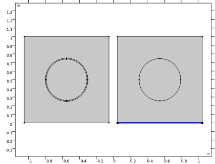
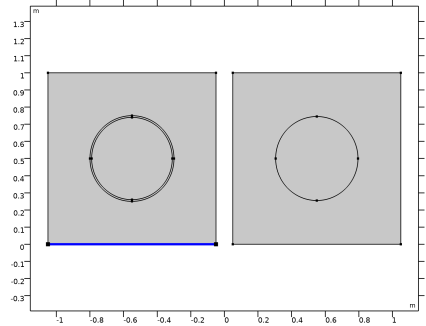
In the Model Builder window, under Component 1 (comp1) right-click Electric Currents (ec) and choose Ground.
2
Ground 2
1
In the Physics toolbar, click  Boundaries and choose Ground.
2
Terminal 1
1
In the Physics toolbar, click  Boundaries and choose Terminal.
2
3
In the Settings window for Terminal, locate the Terminal section.
4
From the Terminal type list, choose Voltage.
Terminal 2
1
In the Physics toolbar, click  Boundaries and choose Terminal.
2
3
In the Settings window for Terminal, locate the Terminal section.
4
From the Terminal type list, choose Voltage.
Electric Shielding 1
1
In the Physics toolbar, click  Boundaries and choose Electric Shielding.
2
In the Settings window for Electric Shielding, locate the Boundary Selection section.
3
From the Selection list, choose Electric Shielding.
Materials
Material 1 (mat1)
1
In the Model Builder window, under Component 1 (comp1) right-click Materials and choose Blank Material.
2
In the Settings window for Material, locate the Geometric Entity Selection section.
3
From the Selection list, choose Bulk.
4
Locate the Material Contents section. In the table, enter the following settings:
Material 2 (mat2)
1
Right-click Materials and choose Blank Material.
2
In the Settings window for Material, locate the Geometric Entity Selection section.
3
From the Selection list, choose Full Fidelity.
4
Locate the Material Contents section. In the table, enter the following settings:
Material 3 (mat3)
1
Right-click Materials and choose Blank Material.
2
In the Settings window for Material, locate the Geometric Entity Selection section.
3
From the Geometric entity level list, choose Boundary.
4
From the Selection list, choose Electric Shielding.
5
Locate the Material Contents section. In the table, enter the following settings:
Mesh 1
In the Model Builder window, under Component 1 (comp1) right-click Mesh 1 and choose Build All.
Study 1
Parametric Sweep
1
In the Study toolbar, click  Parametric Sweep.
2
In the Settings window for Parametric Sweep, locate the Study Settings section.
3
4
5
In the Study toolbar, click  Compute.
Begin the result analysis by excluding the interior of the wall from the selection. The walls interior is not of interest in this comparison.
Results
Study 1/Solution 1 (sol1)
In the Model Builder window, expand the Results>Datasets node, then click Study 1/Solution 1 (sol1).
Selection
1
In the Results toolbar, click  Attributes and choose Selection.
2
In the Settings window for Selection, locate the Geometric Entity Selection section.
3
From the Geometric entity level list, choose Domain.
4
From the Selection list, choose Bulk.
The first default plot shows the electric potential, while the second plot shows the norm of the electric field. Modify the plot group to get a better view on the field shape. Start by disabling the streamlines and adding some contours.
Streamline 1
1
In the Model Builder window, expand the Results>Electric Field Norm (ec) node.
2
Right-click Streamline 1 and choose Disable.
Contour 1
1
In the Model Builder window, right-click Electric Field Norm (ec) and choose Contour.
2
In the Settings window for Contour, click to expand the Title section.
3
From the Title type list, choose None.
4
Locate the Coloring and Style section. From the Coloring list, choose Uniform.
5
From the Color list, choose Gray.
6
Clear the Color legend check box.
Then, add an arrow plot of the electric field.
Arrow Surface 1
1
Right-click Electric Field Norm (ec) and choose Arrow Surface.
2
In the Settings window for Arrow Surface, click Replace Expression in the upper-right corner of the Expression section. From the menu, choose Component 1 (comp1)>Electric Currents>Electric>ec.Ex,ec.Ey - Electric field.
3
Click to expand the Title section. From the Title type list, choose None.
4
Locate the Arrow Positioning section. Find the x grid points subsection. In the Points text field, type 21.
5
Find the y grid points subsection. In the Points text field, type 14.
6
Locate the Coloring and Style section. From the Color list, choose Gray.
7
In the Electric Field Norm (ec) toolbar, click  Plot.
8
Click the  Zoom Extents button in the Graphics toolbar.
Compare the resulting plot with Figure 2.
Electric Field Norm (ec)
1
In the Model Builder window, click Electric Field Norm (ec).
2
In the Settings window for 2D Plot Group, locate the Data section.
3
From the Parameter value (sigma_2 (S/m)) list, choose 10.
4
In the Electric Field Norm (ec) toolbar, click  Plot.
This should look like Figure 3.
Finish by reproducing Figure 4.
5
From the Parameter value (sigma_2 (S/m)) list, choose 0.1.
6
In the Electric Field Norm (ec) toolbar, click  Plot.