PDF

Optical Ring Resonator Notch Filter
Introduction
The simplest optical ring resonator consists of a straight waveguide and a ring waveguide. The two waveguide cores are placed close to each other, so light couples from one waveguide to the other.
When the length of the ring waveguide is a integer number of wavelengths, the ring waveguide is resonant to the wavelength and the light power stored in the ring builds up.
The wave transmitted through the straight waveguide is the interference of the incident wave and the wave that couples over from the ring to the straight waveguide.
Schematically, you can think of the ring resonator as shown in Figure 1 below. A part of the incident wave Ei1 is transmitted in the straight waveguide, whereas a fraction of that field couples over to the ring. Similarly, some of the light in the ring couples over to the straight waveguide, whereas the rest of that wave continuous around the ring waveguide.
Figure 1: Schematic of an optical ring resonator, showing the incident fields Ei1 and Ei2 and the transmitted/coupled fields Et1 and Et2. The transmission and coupling coefficients t and κ are also indicated, as well as the round-trip loss L.
The transmitted fields are related to the incident fields through the matrix-vector relation
(1).
The matrix elements defined above, assures that the total input power equals the total output power,
(2),
by assuming that coupler’s transmission and coupling coefficients are related by
(3).
Furthermore, as the wave propagates around the ring waveguide, you get the relation
(4),
where L is the loss coefficient for the propagation around the ring and is the accumulated phase.
Combining Equation 1, Equation 3 and Equation 4, the transmitted field can be written
(5).
Here the transmission coefficient is separated into the transmission loss |t| and the corresponding phase ,
(6).
Notice, that on resonance, when is an integer number times 2π, and when |t| = L, the transmitted field is zero. The condition that |t| = L is called critical coupling. Thus, when the coupler’s transmission loss balances the loss for the wave propagating around the ring waveguide you get the optimum condition for a bandstop filter, a notch filter.
Model Definition
This application is setup using the Electromagnetic Waves, Beam Envelopes interface, to handle the propagation over distances that are many wavelengths long. Since the wave propagates in essentially one direction along the straight waveguide and along the waveguide ring, the unidirectional formulation is used. This assumes that the electric field for the wave can be written as
(7),
where E1 is a slowly varying field envelope function and is an approximation of the propagation phase for the wave. The definitions used for the phase in the straight and ring waveguide are shown in Table 1 and Table 2.
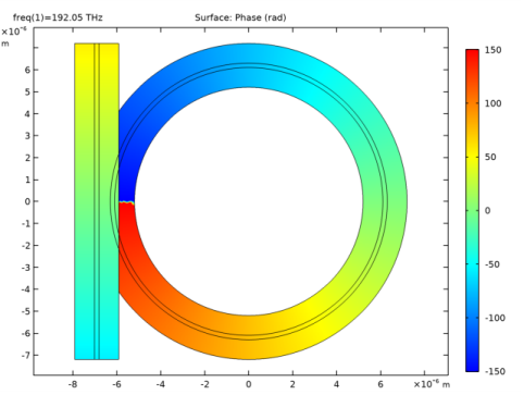
Notice in Figure 2 that the phase approximation defined in Table 1 and in Table 2 is discontinuous at the boundary between the straight waveguide and the ring waveguide. To handle this phase discontinuity and thereby the discontinuity in the field envelope, E1, a Field Continuity boundary condition is used at the boundary between the straight waveguide and the ring waveguide. This boundary condition ensures that the tangential components of the electric and the magnetic fields are continuous at the boundary, despite the phase jump.
Figure 2: Plot of the predefined phase approximation. Notice that the phase jump at y = 0 in the cladding of the left part of the ring waveguide is neglected, as the light is mainly confined to the waveguide core.
Results and Discussion
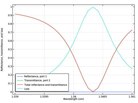
Figure 3 below shows the transmittance spectrum for the optical ring resonator.
Figure 3: Transmittance spectrum for the optical ring resonator.
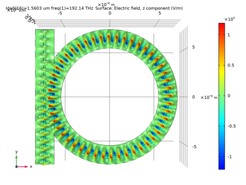
and Figure 4 shows a field plot for a resonant wavelength. Notice that the field in the straight waveguide and the field incoming from the ring is out of phase, when they interfere in the coupler. Thereby the outgoing field in the straight waveguide is almost zero.
Figure 4: The out-of-plane component of the electric field for the resonant wavelength.
Application Library path: Wave_Optics_Module/Waveguides_and_Couplers/optical_ring_resonator
Modeling Instructions
First add the physics interface and the study sequence.
From the File menu, choose New.
New
In the New window, click  Model Wizard.
Model Wizard
1
In the Model Wizard window, click  2D.
2
In the Select Physics tree, select Optics>Wave Optics>Electromagnetic Waves, Beam Envelopes (ewbe).
3
Click Add.
4
Click  Study.
5
In the Select Study tree, select Preset Studies for Selected Physics Interfaces>Boundary Mode Analysis.
6
Geometry 1
The geometry for the optical ring resonator is quite complicated to set up. To get straight to the physics modeling, start by importing the geometry sequence. In the imported MPH-file, the parameters for the geometry are already defined.
1
In the Geometry toolbar, click  Insert Sequence.
2
3
In the Geometry toolbar, click  Build All.
4
Click the  Zoom Extents button in the Graphics toolbar.
Global Definitions
Start by loading a few more parameters required for building the physics and defining the materials.
Parameters 1
1
In the Model Builder window, under Global Definitions click Parameters 1.
2
In the Settings window for Parameters, locate the Parameters section.
3
Click  Load from File.
4
Definitions
Now add the definitions for the phase in the two waveguide domains.
Phase, straight waveguide
1
In the Model Builder window, under Component 1 (comp1) right-click Definitions and choose Variables.
2
In the Settings window for Variables, type Phase, straight waveguide in the Label text field.
3
Locate the Geometric Entity Selection section. From the Geometric entity level list, choose Domain.
4
5
Locate the Variables section. In the table, enter the following settings:
Phase, ring waveguide
1
In the Model Builder window, right-click Definitions and choose Variables.
2
In the Settings window for Variables, type Phase, ring waveguide in the Label text field.
3
Locate the Geometric Entity Selection section. From the Geometric entity level list, choose Domain.
4
5
Locate the Variables section. In the table, enter the following settings:
Materials
Cladding
1
In the Model Builder window, under Component 1 (comp1) right-click Materials and choose Blank Material.
2
In the Settings window for Material, type Cladding in the Label text field.
3
Locate the Material Contents section. In the table, enter the following settings:
Core
1
Right-click Materials and choose Blank Material.
2
In the Settings window for Material, type Core in the Label text field.
3
4
Locate the Material Contents section. In the table, enter the following settings:
Electromagnetic Waves, Beam Envelopes (ewbe)
1
In the Model Builder window, under Component 1 (comp1) click Electromagnetic Waves, Beam Envelopes (ewbe).
2
In the Settings window for Electromagnetic Waves, Beam Envelopes, locate the Wave Vectors section.
3
From the Number of directions list, choose Unidirectional.
4
From the Type of phase specification list, choose User defined.
5
In the φ1 text field, type phi.
Port 1
1
In the Physics toolbar, click  Boundaries and choose Port.
2
3
In the Settings window for Port, locate the Port Properties section.
4
From the Type of port list, choose Numeric.
For the first port, wave excitation is on by default.
Port 2
1
Right-click Port 1 and choose Duplicate.
2
In the Settings window for Port, locate the Boundary Selection section.
3
Click  Clear Selection.
4
5
Locate the Port Properties section. From the Wave excitation at this port list, choose Off.
Scattering Boundary Condition 1
1
In the Physics toolbar, click  Boundaries and choose Scattering Boundary Condition.
2
3
Click the  Show More Options button in the Model Builder toolbar.
4
In the Show More Options dialog box, in the tree, select the check box for the node Physics>Advanced Physics Options.
5
Field Continuity 1
1
In the Physics toolbar, click  Boundaries and choose Field Continuity.
2
Mesh 1
For this model a triangular mesh will be used.
1
In the Model Builder window, under Component 1 (comp1) click Mesh 1.
2
In the Settings window for Mesh, locate the Electromagnetic Waves, Beam Envelopes (ewbe) section.
3
From the Mesh type list, choose Triangular mesh.
4
In the hmax text field, type w_clad/2. This will resolve the cross-section of the wave.
5
Click  Build All.
Study 1
Step 1: Boundary Mode Analysis
1
In the Model Builder window, under Study 1 click Step 1: Boundary Mode Analysis.
2
In the Settings window for Boundary Mode Analysis, locate the Study Settings section.
3
In the Mode analysis frequency text field, type f0.
4
Select the Search for modes around check box.
5
Step 3: Boundary Mode Analysis 1
1
Right-click Study 1>Step 1: Boundary Mode Analysis and choose Duplicate.
2
In the Settings window for Boundary Mode Analysis, locate the Study Settings section.
3
In the Port name text field, type 2.
Step 2: Frequency Domain
1
In the Model Builder window, click Step 2: Frequency Domain.
2
In the Settings window for Frequency Domain, locate the Study Settings section.
3
In the Frequencies text field, type f0.
4
Right-click Study 1>Step 2: Frequency Domain and choose Move Down.
Parametric Sweep
1
In the Study toolbar, click  Parametric Sweep.
2
In the Settings window for Parametric Sweep, locate the Study Settings section.
3
4
From the list in the Parameter name column, choose lda0 (Wavelength).
5
Click  Range.
6
In the Range dialog box, choose Number of values from the Entry method list.
7
In the Start text field, type 1.559[um].
8
In the Stop text field, type 1.561[um].
9
In the Number of values text field, type 25.
10
Click Replace.
11
In the Settings window for Parametric Sweep, locate the Study Settings section.
12
13
In the Study toolbar, click  Compute.
Results
Electric Field
1
In the Model Builder window, expand the Electric Field (ewbe) node, then click Electric Field.
2
In the Settings window for Surface, locate the Expression section.
3
In the Expression text field, type ewbe.Ez.
Height Expression 1
Right-click Electric Field and choose Height Expression.
Electric Field (ewbe)
1
In the Settings window for 2D Plot Group, locate the Data section.
2
From the Parameter value (lda0 (um)) list, choose 1.5603 (1).
3
In the Electric Field (ewbe) toolbar, click  Plot.
4
Click the  Go to XY View button in the Graphics toolbar.
5
Click the  Zoom Extents button in the Graphics toolbar. The plot should now look like Figure 4.
Reflectance, Transmittance, and Loss (ewbe)
For the optical ring resonator, where there is loss due to the propagation in the ring and not due to material absorption, it is more appropriate to use the term loss than absorptance. Thus, replace absorptance with loss in the node label, y-axis label and the legend.
1
In the Model Builder window, under Results click Reflectance, Transmittance, and Absorptance (ewbe).
2
In the Settings window for 1D Plot Group, type Reflectance, Transmittance, and Loss (ewbe) in the Label text field.
3
Locate the Plot Settings section. In the y-axis label text field, type Reflectance, transmittance, and loss.
Global 1
1
In the Model Builder window, expand the Reflectance, Transmittance, and Loss (ewbe) node, then click Global 1.
2
In the Settings window for Global, locate the y-Axis Data section.
3
Reflectance, Transmittance, and Loss (ewbe)
1
In the Model Builder window, click Reflectance, Transmittance, and Loss (ewbe).
2
In the Settings window for 1D Plot Group, locate the Legend section.
3
From the Position list, choose Lower left.
4
In the Reflectance, Transmittance, and Loss (ewbe) toolbar, click  Plot. The plot should now look like Figure 3.