|
|
|
|
1
|
|
2
|
In the Select Physics tree, select Optics>Wave Optics>Electromagnetic Waves, Frequency Domain (ewfd).
|
|
3
|
Click Add.
|
|
4
|
Click
|
|
5
|
|
6
|
Click
|
|
1
|
|
2
|
|
1
|
|
2
|
|
3
|
Click
|
|
4
|
|
5
|
|
6
|
|
7
|
Click Replace.
|
|
1
|
|
2
|
|
3
|
|
1
|
|
2
|
|
1
|
|
2
|
|
1
|
|
2
|
|
1
|
|
2
|
|
3
|
|
1
|
|
2
|
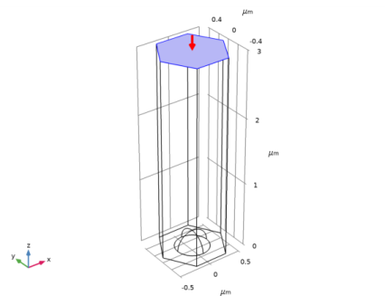
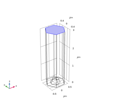
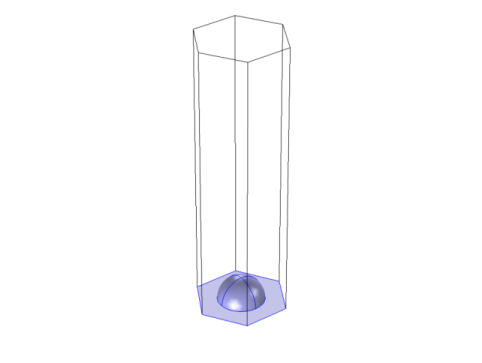
Select the object ext1 only.
|
|
3
|
|
4
|
|
5
|
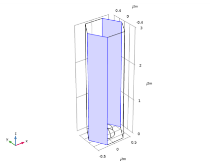
Select the object sph1 only.
|
|
6
|
|
7
|
|
8
|
|
1
|
|
2
|
|
3
|
In the tree, select Built-in>Air.
|
|
4
|
|
5
|
|
1
|
In the Model Builder window, under Component 1 (comp1) right-click Electromagnetic Waves, Frequency Domain (ewfd) and choose Port.
|
|
3
|
|
4
|
|
5
|
|
6
|
|
7
|
In the α2 text field, type phi+pi/3, as this angle is measured from the first side vector of the port (not the x-axis).
|
|
1
|
|
2
|
|
3
|
|
4
|
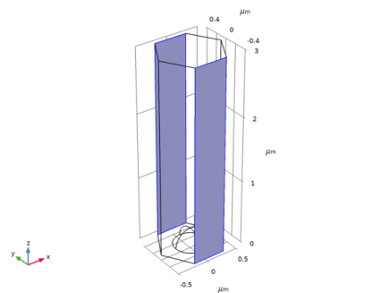
Select Point 2 only. This point selection makes the angle previously provided for alpha_2 consistent with the intended angle of incidence for the incident wave.
 |
|
1
|
|
2
|
|
3
|
|
1
|
|
2
|
|
3
|
|
4
|
|
1
|
|
2
|
|
3
|
|
4
|
|
1
|
|
2
|
|
3
|
|
4
|
|
1
|
|
2
|
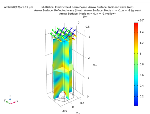
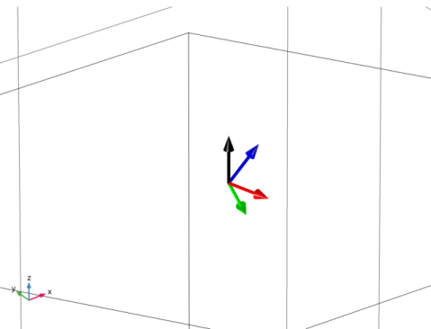
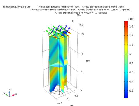
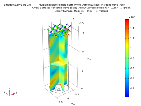
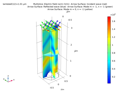
In the Settings window for Arrow Surface, click Replace Expression in the upper-right corner of the Expression section. From the menu, choose Component 1 (comp1)>Electromagnetic Waves, Frequency Domain>Ports>ewfd.kIncx_1,...,ewfd.kIncz_1 - Incident wave vector.
|
|
3
|
|
4
|
In the associated text field, type Incident wave (red).
|
|
1
|
|
2
|
In the Settings window for Arrow Surface, click Replace Expression in the upper-right corner of the Expression section. From the menu, choose Component 1 (comp1)>Electromagnetic Waves, Frequency Domain>Ports>ewfd.kModex_1,...,ewfd.kModez_1 - Port mode wave vector.
|
|
3
|
|
4
|
|
1
|
|
2
|
In the Settings window for Arrow Surface, click Replace Expression in the upper-right corner of the Expression section. From the menu, choose Component 1 (comp1)>Electromagnetic Waves, Frequency Domain>Ports>ewfd.kModex_2,...,ewfd.kModez_2 - Port mode wave vector.
|
|
3
|
|
4
|
|
1
|
|
2
|
In the Settings window for Arrow Surface, click Replace Expression in the upper-right corner of the Expression section. From the menu, choose Component 1 (comp1)>Electromagnetic Waves, Frequency Domain>Ports>ewfd.kModex_4,...,ewfd.kModez_4 - Port mode wave vector.
|
|
3
|
|
4
|
|
1
|
|
2
|
|
3
|
|
4
|
|
5
|
|
1
|
|
2
|
|
3
|
|
4
|
|
5
|
|
6
|
|
1
|
|
2
|
|
3
|
|
4
|
|
5
|
|
6
|
|
7
|
|
8
|
|
9
|
In the tree, select the check box for the node Results>Views.
|
|
10
|
Click OK.
|
|
1
|
|
2
|
Click the Zoom Box button in the Graphics toolbar and then use the mouse to zoom in on the port boundary.
|
|
1
|
|
2
|
|
3
|
|
4
|
|
1
|
|
2
|
|
3
|
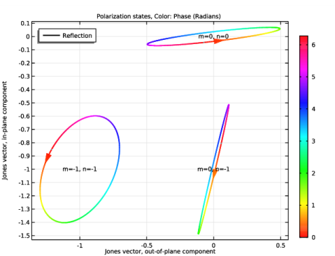
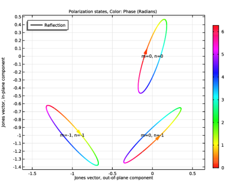
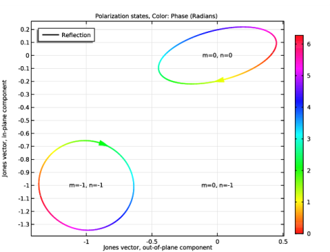
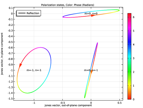
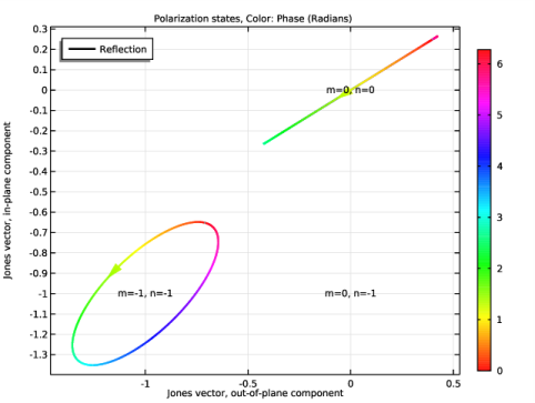
Click Replace Expression in the upper-right corner of the Expression section. From the menu, choose Component 1 (comp1)>Electromagnetic Waves, Frequency Domain>Ports>Polarization state>Jones base vectors>ewfd.eJROOPx_0_0,...,ewfd.eJROOPz_0_0 - Jones base vector on reflection side, out-of-plane direction, order [0,0].
|
|
4
|
|
1
|
|
2
|
|
3
|
Click Replace Expression in the upper-right corner of the Expression section. From the menu, choose Component 1 (comp1)>Electromagnetic Waves, Frequency Domain>Ports>Polarization state>Jones base vectors>ewfd.eJRIPx_0_0,...,ewfd.eJRIPz_0_0 - Jones base vector on reflection side, in-plane direction, order [0,0].
|
|
4
|
|
5
|
|
6
|
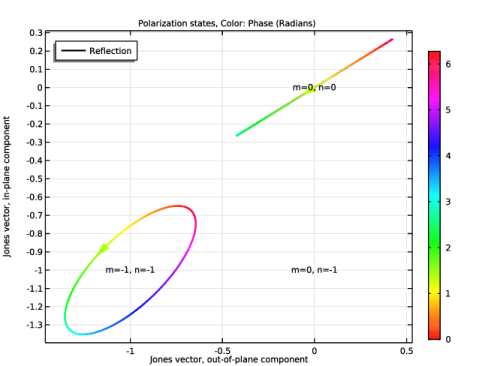
Clear the Color check box.
|
|
1
|
|
2
|
|
3
|
|
4
|
|
5
|
|
6
|
|
1
|
|
2
|
|
1
|
|
1
|
|
2
|
In the Settings window for Arrow Surface, click Replace Expression in the upper-right corner of the Expression section. From the menu, choose Component 1 (comp1)>Electromagnetic Waves, Frequency Domain>Geometry and mesh>ewfd.nx,ewfd.ny,ewfd.nz - Normal vector.
|
|
3
|
|
4
|
|
1
|
|
2
|
|
3
|
|
4
|
|
5
|
|
1
|
|
2
|
|
3
|
|
4
|
|
5
|
|
1
|
|
2
|
|
3
|
|
4
|
|
5
|
|
6
|
|
1
|
In the Model Builder window, under Component 1 (comp1)>Electromagnetic Waves, Frequency Domain (ewfd) click Port 1.
|
|
2
|
|
3
|
|
4
|
|
5
|
|
1
|
|
1
|
|
2
|
|
1
|
|
2
|
|
3
|
|
4
|