PDF

Stress-Optical Effects in a Photonic Waveguide
Introduction
Planar photonic waveguides in silica (SiO2) have great potential for use in wavelength routing applications. The major problem with these kinds of waveguides is birefringence. Anisotropic refractive indices result in fundamental mode splitting and pulse broadening. The goal is to minimize birefringence effects by adapting materials and manufacturing processes. One source of birefringence is the use of a silicon (Si) wafer on which the waveguide structure is deposited. After annealing at high temperature (approximately 1000 °C), mismatch in thermal expansivity between the silica and silicon layers results in thermally induced stresses in the structure at the operating temperature (typically room temperature around 20 °C).
Note: This application requires the Wave Optics Module and the Structural Mechanics Module.
Model Definition
The Stress-Optical Effect
The general linear stress-optical relation can be written, using tensor notation, as
where Δnij = nij  n0 Iij, nij is the refractive index tensor, n0 is the refractive index for a stress-free material, Iij is the identity tensor, Bijkl is the stress-optical tensor, and Skl is the stress tensor. The number of independent parameters in the stress-optical tensor that characterizes this constitutive relation is reduced by symmetry. Because nij and Skl are both symmetric, Bijkl = Bjikl and Bijkl = Bijlk. In many cases it is possible to further reduce the number of independent parameters. The model at hand considers only two independent parameters, B1 and B2. The stress-optical relation then simplifies to
where nx = n11, ny = n22, nz = n33, Sx = S11, Sy = S22, and Sz = S33.
This translates to
Using the two parameters B1 and B2, the model assumes that the nondiagonal parts of nij are negligible.
The first part of this model utilizes the plane strain approximation available in the Solid Mechanics interface. The resulting birefringent refractive index is computed using expression variables and can be considered a postprocessing step of the plane strain model. The refractive index tensor is used as material data for the second part of the model, the mode analysis.
The Application Library model Stress-Optical Effects with Generalized Plane Strain (the model name is stress_optical_generalized) demonstrates a computation, for which the structure is free to bend in the z direction, using a formulation called Generalized Plane Strain.
Electromagnetic Waves
For a given frequency ν, or equivalently, free-space wavelength λ0 = c0/ν, the Wave Optics Module’s Electromagnetic Waves, Frequency Domain interface can be used for the mode analysis. In this model the free-space wavelength is 1.55 μm. The simulation is set up with the electric field components E = (ExEyEz) as dependent variables. The wave is assumed to have the form
and the effective mode index, neff = β/k0, is obtained from the eigenvalues.
For propagating modes it must hold that
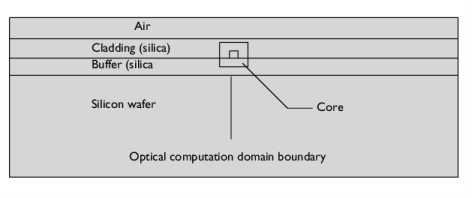
The optical core and planar waveguide layers are made of Silica (SiO2) which is deposited unto a silicon (Si) wafer. The material properties are shown in the following table:
The computational domain can be reduced significantly for the optical mode analysis, because the energy of the fundamental modes is concentrated in the core region and the energy density decays rapidly in the cladding and buffer regions. Thus, you do not need to model the air domain.
Results and Discussion
Figure 1 shows the von Mises stress distribution together with the deformed shape of the waveguide. Notice that the stress varies slowly in the horizontal direction. This means that the significant influence on the stress-induced changes in the refractive index comes from the stress variations in the vertical direction. This is expected because the extension of the domains in the x direction is chosen to minimize the effects of the edges.
Figure 1: von Mises equivalent stress.
Figure 2 shows the birefringence, nx − ny, in the optical computation domain. The birefringence is nearly constant along any horizontal line, so the influence of the side edges is indeed reduced to a minimum.
Figure 2: Birefringence.
Figure 3 shows the effective mode indices for the first four propagating modes. The value para = 0 corresponds to the case without stress-optical effect, while this effect is included for para = 1.
The difference is significant, which shows that the shift in the effective mode indices due to the stress-optical effect is indeed resolved.
The computations show a shift in effective mode index due to the stress-induced change in refractive index. The birefringence causes the otherwise two-fold degenerate fundamental mode to split.
Figure 3: Effective mode indices for the first four propagating modes without (para = 0) and with (para = 1) the stress-optical effect.
Figure 4 shows the out-of-plane component (z component) of the Poynting vector for four eigenmodes computed without the stress-optical coupling.
Figure 4: Eigenmodes computed without the stress-optical coupling.
Visual inspection of the higher eigenmodes indicates that they have a larger portion of energy leaking into the cladding and buffer, and are thus more affected than the fundamental modes by the distance to the air and silicon layers. Because of this leakage, the boundary condition affects the higher eigenmodes more than the fundamental mode.
The change in the eigenmodes shape due to the stress-optical effect is shown in Figure 5.
Figure 5: Eigenmodes computed with the stress-optical effect taken into account.
Although the fundamental modes have converged to 5 decimal places, the known modeling errors makes the exactness of the numbers uncertain. One major modeling error is due to the fact that the model contains a plane strain assumption in a case where the real-world model does not necessarily conform to this deformation state. This modeling error is reduced in the refined model Stress-Optical Effects with Generalized Plane Strain (the model name is stress_optical_generalized).
References
1. H.P. Schriemer and M. Cada, “Modal birefringence and power density distribution in strained buried-core square waveguides,” IEEE Journal of Quantum Electronics, vol. 40, pp. 1131–1139, 2004.
2. J. Stone, “Stress-Optic Effects, Birefringence, and Reduction of Birefringence by Annealing in Fiber Fabry-Perot Interferometers,” J. Lightwave Technol., vol. 6, pp. 1245–1248, 1988.
Application Library path: Structural_Mechanics_Module/Stress_Optical_Effects/stress_optical
Modeling Instructions
From the File menu, choose New.
New
In the New window, click  Model Wizard.
Model Wizard
1
In the Model Wizard window, click  2D.
2
In the Select Physics tree, select Structural Mechanics>Solid Mechanics (solid).
3
Click Add.
4
In the Select Physics tree, select Optics>Wave Optics>Electromagnetic Waves, Frequency Domain (ewfd).
5
Click Add.
6
Click  Study.
7
In the Select Study tree, select Preset Studies for Some Physics Interfaces>Stationary.
8
Global Definitions
Parameters 1
1
In the Model Builder window, under Global Definitions click Parameters 1.
2
In the Settings window for Parameters, locate the Parameters section.
3
Click  Load from File.
4
Add a parameter to switch the stress effects on and off.
5
Geometry 1
1
In the Model Builder window, under Component 1 (comp1) click Geometry 1.
2
In the Settings window for Geometry, locate the Units section.
3
From the Length unit list, choose µm.
Rectangle 1 (r1)
1
In the Geometry toolbar, click  Rectangle.
2
In the Settings window for Rectangle, locate the Size and Shape section.
3
In the Width text field, type 320.
4
In the Height text field, type 83.
5
Locate the Position section. In the x text field, type -160.
6
In the y text field, type -100.
Rectangle 2 (r2)
1
In the Geometry toolbar, click  Rectangle.
2
In the Settings window for Rectangle, locate the Size and Shape section.
3
In the Width text field, type 320.
4
In the Height text field, type 14.
5
Locate the Position section. In the x text field, type -160.
6
In the y text field, type -17.
Rectangle 3 (r3)
1
In the Geometry toolbar, click  Rectangle.
2
In the Settings window for Rectangle, locate the Size and Shape section.
3
In the Width text field, type 320.
4
In the Height text field, type 16.
5
Locate the Position section. In the x text field, type -160.
6
In the y text field, type -3.
Rectangle 4 (r4)
1
In the Geometry toolbar, click  Rectangle.
2
In the Settings window for Rectangle, locate the Size and Shape section.
3
In the Width text field, type 6.
4
In the Height text field, type 6.
5
Locate the Position section. In the x text field, type -3.
6
In the y text field, type -3.
Rectangle 5 (r5)
1
In the Geometry toolbar, click  Rectangle.
2
In the Settings window for Rectangle, locate the Size and Shape section.
3
In the Width text field, type 20.
4
In the Height text field, type 20.
5
Locate the Position section. In the x text field, type -10.
6
In the y text field, type -10.
7
Click  Build Selected.
The last rectangular region encloses the optical computational domain. It can be enlarged if needed for validating the results. The region should be chosen large enough so that the computed propagation constants do not change significantly if the region is enlarged.
Solid Mechanics (solid)
Linear Elastic Material 1
In the Model Builder window, under Component 1 (comp1)>Solid Mechanics (solid) click Linear Elastic Material 1.
Thermal Expansion 1
1
In the Physics toolbar, click  Attributes and choose Thermal Expansion.
2
In the Settings window for Thermal Expansion, locate the Model Input section.
3
From the T list, choose User defined. In the associated text field, type T1.
4
Click  Go to Source.
Global Definitions
Default Model Inputs
1
In the Model Builder window, under Global Definitions click Default Model Inputs.
2
In the Settings window for Default Model Inputs, locate the Browse Model Inputs section.
3
Find the Expression for remaining selection subsection. In the Volume reference temperature text field, type T0.
Definitions
Variables 1
1
In the Home toolbar, click  Variables and choose Local Variables.
2
In the Settings window for Variables, locate the Variables section.
3
4
Locate the Geometric Entity Selection section. From the Geometric entity level list, choose Domain.
5
Variables 2
1
In the Home toolbar, click  Variables and choose Local Variables.
2
In the Settings window for Variables, locate the Variables section.
3
4
Locate the Geometric Entity Selection section. From the Geometric entity level list, choose Domain.
5
Variables 3
1
In the Home toolbar, click  Variables and choose Local Variables.
2
In the Settings window for Variables, locate the Variables section.
3
4
Locate the Geometric Entity Selection section. From the Geometric entity level list, choose Domain.
5
Solid Mechanics (solid)
All regions have free boundaries, which also is the default boundary condition. However, these conditions will not be sufficient for creating a unique solution because the computational domain is allowed to move and rotate freely. The problem becomes well-posed by adding constraints to restrain such rigid body movements.
Rigid Motion Suppression 1
1
In the Physics toolbar, click  Domains and choose Rigid Motion Suppression.
2
Electromagnetic Waves, Frequency Domain (ewfd)
The computational domain is reduced significantly for the optical mode analysis.
1
In the Model Builder window, under Component 1 (comp1) click Electromagnetic Waves, Frequency Domain (ewfd).
2
Wave Equation, Electric 1
1
In the Model Builder window, under Component 1 (comp1)>Electromagnetic Waves, Frequency Domain (ewfd) click Wave Equation, Electric 1.
2
In the Settings window for Wave Equation, Electric, locate the Electric Displacement Field section.
3
From the n list, choose User defined. From the list, choose Diagonal.
4
In the n table, enter the following settings:
5
From the k list, choose User defined.
Materials
Si
1
In the Model Builder window, under Component 1 (comp1) right-click Materials and choose Blank Material.
2
In the Settings window for Material, type Si in the Label text field.
3
4
Locate the Material Contents section. In the table, enter the following settings:
SiO2
1
Right-click Materials and choose Blank Material.
2
In the Settings window for Material, type SiO2 in the Label text field.
3
4
Locate the Material Contents section. In the table, enter the following settings:
Mesh 1
Free Triangular 1
In the Mesh toolbar, click  Free Triangular.
Size 1
1
Right-click Free Triangular 1 and choose Size.
2
In the Settings window for Size, locate the Geometric Entity Selection section.
3
From the Geometric entity level list, choose Domain.
4
5
Locate the Element Size section. Click the Custom button.
6
Locate the Element Size Parameters section. Select the Maximum element size check box.
7
Size
1
In the Model Builder window, click Size.
2
In the Settings window for Size, locate the Element Size section.
3
From the Predefined list, choose Extra fine.
4
Click  Build All.
Study 1
Mode Analysis
1
In the Study toolbar, click  Study Steps and choose Other>Mode Analysis.
2
In the Settings window for Mode Analysis, locate the Study Settings section.
3
From the Transform list, choose Effective mode index.
4
In the Search for modes around text field, type 1.46.
5
Select the Desired number of modes check box.
6
7
In the Mode analysis frequency text field, type c_const/lambda0_ewfd.
These settings make the eigenmode solver search for the 4 eigenmodes with effective mode indices closest to the value 1.46. This value is an estimate of the effective mode index for the fundamental mode.
Exclude Solid Mechanics from the Mode Analysis step.
8
Locate the Physics and Variables Selection section. In the table, clear the Solve for check box for Solid Mechanics (solid).
Step 1: Stationary
1
In the Model Builder window, click Step 1: Stationary.
2
In the Settings window for Stationary, locate the Physics and Variables Selection section.
3
In the table, clear the Solve for check box for Electromagnetic Waves, Frequency Domain (ewfd).
Parametric Sweep
1
In the Study toolbar, click  Parametric Sweep.
2
In the Settings window for Parametric Sweep, locate the Study Settings section.
3
4
5
In the Study toolbar, click  Compute.
Results
Stress (solid)
1
In the Settings window for 2D Plot Group, locate the Data section.
2
From the Dataset list, choose Study 1/Solution Store 1 (sol2).
3
In the Stress (solid) toolbar, click  Plot.
4
Click the  Zoom Extents button in the Graphics toolbar.
To visualize the details of the eigenmodes, you first set up a view that includes the optical computation domain only.
5
Click the  Show More Options button in the Model Builder toolbar.
6
In the Show More Options dialog box, in the tree, select the check box for the node Results>Views.
7
View 2D 2
1
In the Model Builder window, right-click Views and choose View 2D.
2
In the Settings window for View 2D, locate the View section.
3
Select the Lock axis check box.
Axis
1
In the Model Builder window, expand the View 2D 2 node, then click Axis.
2
In the Settings window for Axis, locate the Axis section.
3
In the x minimum text field, type -11.
4
In the x maximum text field, type 11.
5
In the y minimum text field, type -11.
6
In the y maximum text field, type 11.
Electric Field (ewfd)
1
In the Model Builder window, click Electric Field (ewfd).
2
In the Settings window for 2D Plot Group, locate the Plot Settings section.
3
From the View list, choose View 2D 2.
Surface 1
1
In the Model Builder window, expand the Electric Field (ewfd) node, then click Surface 1.
2
In the Settings window for Surface, click Replace Expression in the upper-right corner of the Expression section. From the menu, choose Component 1 (comp1)>Electromagnetic Waves, Frequency Domain>Energy and power>Power flow, time average (spatial frame) - W/m²>ewfd.Poavz - Power flow, time average, z component.
Electric Field (ewfd)
1
In the Model Builder window, click Electric Field (ewfd).
2
In the Settings window for 2D Plot Group, locate the Data section.
3
From the Parameter value (para) list, choose 0.
4
In the Electric Field (ewfd) toolbar, click  Plot. This creates a visualization of the power flow, also called optical intensity or the Poynting vector, in the z direction (out-of-plane direction). Continue to plot the power flow for the other computed eigenmodes, with and without stress effects.
2D Plot Group 3
Next, plot the birefringence Nx-Ny in the waveguide.
1
In the Home toolbar, click  Add Plot Group and choose 2D Plot Group.
2
In the Settings window for 2D Plot Group, locate the Data section.
3
From the Dataset list, choose Study 1/Solution Store 1 (sol2).
4
Locate the Plot Settings section. From the View list, choose View 2D 2.
5
Click to expand the Title section. From the Title type list, choose Manual.
6
In the Title text area, type Surface: Nx-Ny.
Surface 1
1
Right-click 2D Plot Group 3 and choose Surface.
2
In the Settings window for Surface, locate the Expression section.
3
In the Expression text field, type Nx-Ny.
4
In the 2D Plot Group 3 toolbar, click  Plot.
Global Evaluation 1
To collect all computed effective mode indices in a table, follow these steps:
1
In the Results toolbar, click  Global Evaluation.
2
In the Settings window for Global Evaluation, locate the Data section.
3
From the Dataset list, choose Study 1/Parametric Solutions 1 (sol3).
4
From the Table columns list, choose Inner solutions.
5
Click Replace Expression in the upper-right corner of the Expressions section. From the menu, choose Component 1 (comp1)>Electromagnetic Waves, Frequency Domain>Global>ewfd.neff - Effective mode index.
6
Click  Evaluate.
Table
1
Go to the Table window.
If you see too few digits in the table, click the Full Precision toolbar button.
Results
Finally, create a table plot to visualize the split of the effective mode indices.
1D Plot Group 4
In the Results toolbar, click  1D Plot Group.
Table Graph 1
1
Right-click 1D Plot Group 4 and choose Table Graph.
2
In the Settings window for Table Graph, locate the Coloring and Style section.
3
Find the Line style subsection. From the Line list, choose Dashed.
4
Find the Line markers subsection. From the Marker list, choose Circle.
1D Plot Group 4
1
In the Model Builder window, click 1D Plot Group 4.
2
In the Settings window for 1D Plot Group, click to expand the Title section.
3
From the Title type list, choose Manual.
4
In the Title text area, type Eigenvalue shift.
5
Locate the Axis section. Select the Manual axis limits check box.
6
In the x minimum text field, type 0.
7
In the x maximum text field, type 1.
8
In the y minimum text field, type 1.443.
9
In the y maximum text field, type 1.453.
10
Locate the Grid section. Select the Manual spacing check box.
11
In the y spacing text field, type 1e-3.
12
In the 1D Plot Group 4 toolbar, click  Plot.