PDF

Si Solar Cell 1D
This tutorial uses a simple 1D model of a silicon solar cell to illustrate the basic steps to set up and perform a semiconductor simulation with the COMSOL Semiconductor Module.
Introduction
The solar cell model consists of a 1D silicon p-n junction with carrier generation and Shockley-Read-Hall recombination.
The p-n junction is formed by p-doping the front surface of an n-type Si wafer. The uniform bulk n-doping is assumed to be 1·1016 cm3. The front surface p-doping is assumed to have a peak concentration of 1·1019 cm3, and a Gaussian drop off with a junction depth of 0.25 μm.
The carrier generation mechanism from the photovoltaic effect is not modeled in detail. Instead, for simplicity, a user-defined spatially dependent variable is created for the generation rate, using an integral expression involving the solar irradiance and silicon absorption spectra. In addition, the Shockley-Read-Hall model is employed to capture the main recombination effect.
Under normal operating conditions, photo-generated carriers are swept to each side of the depletion region of the p-n junction. A small forward bias voltage is applied to extract the electrical power, given by the product of the photocurrent and the applied voltage.
Model Definition
This model simulates the behavior of the solar cell under forward bias with a voltage between 0 and 0.61 V. The modeled domain has a thickness of 150 μm. The built-in Si material data is assumed.
An Analytic Doping Model feature is used for the uniform bulk doping and a Geometric Doping Model is used for the front surface doping (the surface is specified in the Boundary Selection for Doping Profile subnode).
The Shockley-Read-Hall recombination model is implemented in a Trap-Assisted Recombination feature, and the photo-generation is done in a User-Defined Generation feature. The electrical connections to the front and back surfaces are done with two Metal Contact features.
The integral expression for the photo-generation rate is shown below
(1)
where z is the depth into the device from the surface, λ is the wavelength, α(λ) is the absorption coefficient defined by
(2)
where κ(λ) is the imaginary part of the refractive index (data given by Ref. 2), and is the photon generation rate defined by
(3)
where F(λ) is the spectral irradiance (here approximated by the AM 1.5 spectrum given by Ref. 3)
The mesh is adjusted from the default in order to resolve the steep gradients near the surface of the relatively thick device. The voltage sweep is done using a Stationary study with Auxiliary sweep enabled, using the solution from a Semiconductor Equilibrium study step as the initial condition.
Results and Discussion
Figure 1shows the donor and acceptor concentrations for the depths of first 10 μm beneath the front surface. It is always a good idea to check the doping profile for unintentional setup errors.
.
Figure 1: Donor and acceptor concentrations for the depths of first 10 mm beneath the front surface
Figure 2 shows the Shockley-Read-Hall recombination rate and the user-defined photo-generation rate throughout the thickness of the cell.
Figure 2: Shockley-Read-Hall recombination rate and user-defined photo-generation rate throughout the thickness of the cell.
Figure 3 and Figure 4 show the I-V and P-V curves. These graphs allow us to read off essential operating parameters such as the open circuit voltage (~0.61 V), the short circuit current (~33 mA), and the max power (~16.7 mW).
Figure 3: I-V curve of the solar cell
.
Figure 4: P-V curve of the cell.
References
1. The Photovoltaic Education Network, http://pveducation.org.
2. http://refractiveindex.info/?shelf=main&book=Si&page=Green-2008
3. http://rredc.nrel.gov/solar/spectra/am1.5/
Application Library path: Semiconductor_Module/Photonic_Devices_and_Sensors/si_solar_cell_1d
Modeling Instructions
From the File menu, choose New.
New
In the New window, click  Model Wizard.
Model Wizard
1
In the Model Wizard window, click  1D.
2
In the Select Physics tree, select Semiconductor>Semiconductor (semi).
3
Click Add.
4
Click  Study.
We will start with the Semiconductor Equilibrium study type, which often helps us find a good initial condition for subsequent study steps.
5
In the Select Study tree, select Preset Studies for Selected Physics Interfaces>Semiconductor Equilibrium.
6
Start by creating a global parameter for the applied voltage. Global parameters are independent of space and time in a model.
Global Definitions
Parameters 1
1
In the Model Builder window, under Global Definitions click Parameters 1.
2
In the Settings window for Parameters, locate the Parameters section.
3
Create a simple geometry, using um as the length unit for convenience.
Geometry 1
1
In the Model Builder window, under Component 1 (comp1) click Geometry 1.
2
In the Settings window for Geometry, locate the Units section.
3
From the Length unit list, choose µm.
Interval 1 (i1)
1
Right-click Component 1 (comp1)>Geometry 1 and choose Interval.
2
In the Settings window for Interval, locate the Interval section.
3
4
In the Home toolbar, click  Build All.
Define functions and variables for the spectra and generation rate of the charge carriers. First, for the solar spectrum, we use a rough approximation of the Reference AM 1.5 Spectra, the original data of which is available from Ref. 3. The unit of this function is irradiance per wavelength, or power per area per wavelength (W/m^2/nm).
Global Definitions
Interpolation 1: solar spectrum
1
In the Home toolbar, click  Functions and choose Global>Interpolation.
2
In the Settings window for Interpolation, type Interpolation 1: solar spectrum in the Label text field.
3
Locate the Definition section. From the Data source list, choose File.
4
Click Browse.
5
6
Find the Functions subsection. In the table, enter the following settings:
7
Locate the Units section. In the Arguments text field, type nm.
8
In the Function text field, type W/m^2/nm.
9
Locate the Definition section. Click Import.
For the silicon absorption spectrum, import a file that has two output columns, one for the refractive index n and the other for the extinction coefficient k. The original data is available from Ref. 2.
Interpolation 2: Si absorption spectrum
1
In the Home toolbar, click  Functions and choose Global>Interpolation.
2
In the Settings window for Interpolation, type Interpolation 2: Si absorption spectrum in the Label text field.
3
Locate the Definition section. From the Data source list, choose File.
4
Click Browse.
5
6
In the Number of arguments text field, type 1.
7
Find the Functions subsection. In the table, enter the following settings:
8
Locate the Units section. In the Arguments text field, type um.
9
In the Function text field, type 1.
10
Locate the Definition section. Click Import.
Definitions
Finally add a variable for the photo-generation rate. Variables can in general depend on space and time. Here we will use the stationary study to solve for the steady state, so the generation rate is spatially dependent and time independent. The solar and silicon spectra are used in the integral over the range of wavelengths where both the irradiance on Earth and the absorption in silicon are significant.
Variables 1: Photogeneration
1
In the Model Builder window, under Component 1 (comp1) right-click Definitions and choose Variables.
2
In the Settings window for Variables, type Variables 1: Photogeneration in the Label text field.
3
Locate the Geometric Entity Selection section. From the Geometric entity level list, choose Domain.
4
From the Selection list, choose All domains.
5
Locate the Variables section. In the table, enter the following settings:
Add the built-in silicon material.
Add Material
1
In the Home toolbar, click  Add Material to open the Add Material window.
2
Go to the Add Material window.
3
In the tree, select Semiconductors>Si - Silicon.
4
Click Add to Component in the window toolbar.
5
In the Home toolbar, click  Add Material to close the Add Material window.
Set up domain and boundary conditions for the physics.
Semiconductor (semi)
1
In the Model Builder window, under Component 1 (comp1) click Semiconductor (semi).
2
In the Settings window for Semiconductor, locate the Cross-Section Area section.
3
In the A text field, type 1[cm^2].
4
Locate the Model Properties section. From the Carrier statistics list, choose Fermi-Dirac.
Add a uniform bulk doping.
Analytic Doping Model 1
1
In the Physics toolbar, click  Domains and choose Analytic Doping Model.
2
In the Settings window for Analytic Doping Model, locate the Domain Selection section.
3
From the Selection list, choose All domains.
4
Locate the Impurity section. From the Impurity type list, choose Donor doping (n-type).
Then add a Gaussian doping decaying away from the surface of the device to form the p-n junction. The Geometric Doping Model is convenient for setting up this kind of doping profiles. Remember to make a selection of the boundary for the subnode Boundary Selection for Doping Profile.
Geometric Doping Model 1
1
In the Physics toolbar, click  Domains and choose Geometric Doping Model.
2
In the Settings window for Geometric Doping Model, locate the Domain Selection section.
3
From the Selection list, choose All domains.
4
Locate the Impurity section. In the NA0 text field, type 1e19[1/cm^3].
5
Locate the Profile section. In the dj text field, type 0.25[um].
6
From the Nb list, choose Donor concentration (semi/adm1).
Boundary Selection for Doping Profile 1
1
In the Model Builder window, expand the Geometric Doping Model 1 node, then click Boundary Selection for Doping Profile 1.
2
Add Shockley-Read-Hall recombination using default parameters for silicon.
Trap-Assisted Recombination 1
1
In the Physics toolbar, click  Domains and choose Trap-Assisted Recombination.
2
In the Settings window for Trap-Assisted Recombination, locate the Domain Selection section.
3
From the Selection list, choose All domains.
Add the photo-generation and use the spatially varying variable defined above for the generation rate.
User-Defined Generation 1
1
In the Physics toolbar, click  Domains and choose User-Defined Generation.
2
In the Settings window for User-Defined Generation, locate the Domain Selection section.
3
From the Selection list, choose All domains.
4
Locate the User-Defined Generation section. In the Gn,0 text field, type G_ph.
5
In the Gp,0 text field, type G_ph.
Add two metal contacts with one grounded and the other a voltage applied.
Metal Contact 1
1
In the Physics toolbar, click  Boundaries and choose Metal Contact.
2
Metal Contact 2
1
In the Physics toolbar, click  Boundaries and choose Metal Contact.
2
3
In the Settings window for Metal Contact, locate the Terminal section.
4
In the V0 text field, type V0.
The modeling domain is quite large compared to the length scale of the steep gradients of physical quantities near the surface of the device. So we will adjust the mesh in order to resolve the gradients.
Mesh 1
1
In the Model Builder window, under Component 1 (comp1) click Mesh 1.
2
In the Settings window for Mesh, locate the Physics-Controlled Mesh section.
3
From the Element size list, choose Finer.
Size
Right-click Component 1 (comp1)>Mesh 1 and choose Edit Physics-Induced Sequence.
Size 1
1
2
In the Settings window for Size, click to expand the Element Size Parameters section.
3
Locate the Element Size section. Click the Custom button.
4
Locate the Element Size Parameters section. Select the Maximum element size check box.
5
Add a Stationary study step to sweep the applied voltage.
Study 1
Stationary
1
In the Study toolbar, click  Study Steps and choose Stationary>Stationary.
2
In the Settings window for Stationary, click to expand the Study Extensions section.
3
Select the Auxiliary sweep check box.
4
5
6
In the Study toolbar, click  Compute.
Results
Doping
1
In the Home toolbar, click  Add Plot Group and choose 1D Plot Group.
2
In the Settings window for 1D Plot Group, type Doping in the Label text field.
3
Locate the Data section. From the Parameter selection (V0) list, choose First.
Line Graph 1
1
Right-click Doping and choose Line Graph.
2
In the Settings window for Line Graph, locate the Selection section.
3
From the Selection list, choose All domains.
4
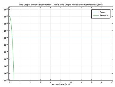
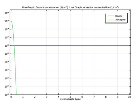
Click Replace Expression in the upper-right corner of the y-Axis Data section. From the menu, choose Component 1 (comp1)>Semiconductor>Carriers and dopants>Dopant concentrations>semi.Nd - Donor concentration - 1/m³.
5
Locate the y-Axis Data section. In the Unit field, type 1/cm^3.
6
Locate the x-Axis Data section. From the Parameter list, choose Expression.
7
In the Expression text field, type x.
8
Click to expand the Legends section. Select the Show legends check box.
9
From the Legends list, choose Manual.
10
Line Graph 2
1
Right-click Line Graph 1 and choose Duplicate.
2
In the Settings window for Line Graph, locate the y-Axis Data section.
3
In the Expression text field, type semi.Na.
4
Locate the Legends section. In the table, enter the following settings:
5
In the Doping toolbar, click  Plot.
6
Click the  y-Axis Log Scale button in the Graphics toolbar.
Zoom in to show the doping profile near the surface in more detail.
Doping
1
In the Model Builder window, click Doping.
2
In the Settings window for 1D Plot Group, locate the Axis section.
3
Select the Manual axis limits check box.
4
In the x minimum text field, type -0.1.
5
In the x maximum text field, type 10.1.
6
In the y minimum text field, type 1e10.
7
In the Doping toolbar, click  Plot.
Plot the generation and recombination rates.
Generation/Recombination rates
1
Right-click Doping and choose Duplicate.
2
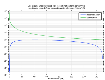
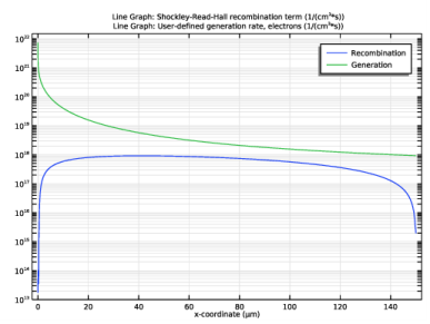
In the Settings window for 1D Plot Group, type Generation/Recombination rates in the Label text field.
3
Locate the Axis section. Clear the Manual axis limits check box.
Line Graph 1
1
In the Model Builder window, expand the Generation/Recombination rates node, then click Line Graph 1.
2
In the Settings window for Line Graph, click Replace Expression in the upper-right corner of the y-Axis Data section. From the menu, choose Component 1 (comp1)>Semiconductor>Generation and recombination>semi.Rsrh - Shockley-Read-Hall recombination term - 1/(m³·s).
3
Locate the y-Axis Data section. In the Unit field, type 1/(cm^3*s).
4
Locate the Legends section. In the table, enter the following settings:
Line Graph 2
In the Model Builder window, right-click Line Graph 2 and choose Delete.
Line Graph 2
1
In the Model Builder window, under Results>Generation/Recombination rates right-click Line Graph 1 and choose Duplicate.
2
In the Settings window for Line Graph, click Replace Expression in the upper-right corner of the y-Axis Data section. From the menu, choose Component 1 (comp1)>Semiconductor>Generation and recombination>semi.udg1.Gn - User-defined generation rate, electrons - 1/(m³·s).
3
Locate the Legends section. In the table, enter the following settings:
4
In the Generation/Recombination rates toolbar, click  Plot.
Generation/Recombination rates
1
In the Model Builder window, click Generation/Recombination rates.
2
In the Settings window for 1D Plot Group, locate the Axis section.
3
Select the Manual axis limits check box.
4
In the y minimum text field, type 1e13.
5
In the Generation/Recombination rates toolbar, click  Plot.
Plot the I-V curve.
I-V curve
1
In the Home toolbar, click  Add Plot Group and choose 1D Plot Group.
2
In the Settings window for 1D Plot Group, type I-V curve in the Label text field.
3
Locate the Legend section. Clear the Show legends check box.
Global 1
1
Right-click I-V curve and choose Global.
2
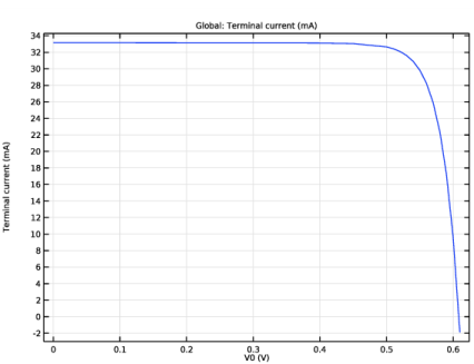
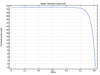
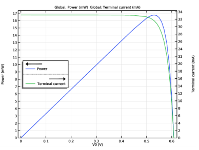
In the Settings window for Global, click Replace Expression in the upper-right corner of the y-Axis Data section. From the menu, choose Component 1 (comp1)>Semiconductor>Terminals>semi.I0_1 - Terminal current - A.
3
Locate the y-Axis Data section. In the table, enter the following settings:
4
In the I-V curve toolbar, click  Plot.
Plot the P-V curve.
P-V curve
1
In the Model Builder window, right-click I-V curve and choose Duplicate.
2
In the Model Builder window, click I-V curve 1.
3
In the Settings window for 1D Plot Group, type P-V curve in the Label text field.
Global 1
1
In the Model Builder window, click Global 1.
2
In the Settings window for Global, locate the y-Axis Data section.
3
P-V curve
1
In the Model Builder window, click P-V curve.
2
In the P-V curve toolbar, click  Plot.
The I-V and P-V curves can be combined in a single figure, by copying the I-V plot into this plot group. The scales of the two curves can be separated by using the Two y-axes option.
Global 1
In the Model Builder window, right-click Global 1 and choose Copy.
Global 2
In the Model Builder window, right-click P-V curve and choose Paste Global.
P-V and I-V curves
1
In the Settings window for 1D Plot Group, type P-V and I-V curves in the Label text field.
2
Locate the Plot Settings section. Select the Two y-axes check box.
3
In the table, select the Plot on secondary y-axis check box for Global 2.
4
Click the  Zoom Extents button in the Graphics toolbar.
5
Locate the Axis section. Select the Manual axis limits check box.
6
In the y minimum text field, type 0.
7
In the Secondary y minimum text field, type 0.
8
Locate the Legend section. Select the Show legends check box.
9
From the Position list, choose Middle left.
10
In the P-V and I-V curves toolbar, click  Plot.