Previous PDF

Interface Trapping Effects of a MOSCAP
This tutorial compares experimental data from the literature with a COMSOL model of a MOSCAP with interface traps (surface states). The Trap-Assisted Surface Recombination feature is used to simulate the effects of the trap charges and the processes of carrier capturing and emitting by the traps. The effect of the fixed charges in the gate oxide is also included. The computed values of the capacitance and conductance as functions of the gate voltage and frequency reproduce the qualitative behavior of the experimental data with comparable magnitudes. The model uses the quasi-Fermi level formulation and shows how to plot quantities such as the trap occupancy as a function of the energy.
Introduction
The metal-silicon-oxide (MOS) structure is the fundamental building block for many silicon planar devices. In a practical interface between the silicon and the oxide, defects and dangling bonds form interface traps (surface states) that can affect the charge transport by capturing and emitting carriers, and can affect the electrostatics via the net surface charge density of the traps. In addition, fixed charges in the oxide also affect the electrostatics. This tutorial constructs a simple 1D model of a MOS capacitor (MOSCAP) to explore these effects and compare with experimental observations.
Model Definition
The 1D MOSCAP model is based on the experimental device (the n-type sample) described in Fig. 14 of Ref. 1. The simulation parameters are taken from the nominal experimental values whenever possible, as detailed below.
The experimental samples were prepared with a 10 μm thick epitaxial layer grown on low-resistivity substrates to minimize the effect of the bulk series resistance. In the model the epilayer is assume to be the same thickness (10 μm), and the substrate is 2 μm thick, assuming the bulk series resistance can be ignored. The oxide thickness is assumed to be 60 nm, in the middle of the experimental range of 50~70 nm. The diameter of the gate is 3.8·102 cm as given in the figure caption.
The electron mobility is assumed to be constant 1450 cm2/V/s. The n-doping concentrations in the epilayer and the substrate are then computed from the experimental values of resistivity of 0.75 and 0.005 ohm-cm, respectively.
The oxide dielectric constant is assumed to be 3.9. The oxide capacitance is then computed from its dielectric constant, thickness, and the gate diameter.
The fixed oxide charge density is 9·1011 cm2 as given by the reference paper.
The trap energy distribution is assumed to be rectangular, with a range of 0.2 eV, centered around the mid-gap. The height of the rectangle is assumed to be 2·1011 cm2eV1, as suggested by Fig. 15 of the reference paper. For the capture process, the thermal velocity is assumed to be 107 cm/s, and the cross sections are 1·10-15 cm2 and 2.2·10-16 cm2 for the electrons and holes, respectively, as given on the same page as Fig. 15 of the paper.
The metal work function of the gate is assumed to be 4.5 eV.
Results and Discussion
Figure 1 shows the computed terminal capacitance and the equivalent parallel conductance as functions of the gate voltage to compare with Fig. 23 in Ref. 1. The curves show the same qualitative behavior with comparable magnitudes.
Figure 1: Cm-V and Gp-V curves.
Figure 2 shows the computed terminal capacitance and the equivalent parallel conductance as functions of the small signal frequency. The qualitative behavior of the equivalent parallel conductance compares well with Fig. 25 in Ref. 1 (The paper did not include capacitance in the figure.)
Figure 2: Cm and Gp vs. frequency.
Figure 3 shows the rectangular density of states for the traps.
Figure 3: Density of trap states along the energy axis.
Figure 4 and Figure 5 shows the trap occupancy to gain some insight on the effect of the traps on the Cm-V and Gp-V curves. See the discussions in the section Modeling Instructions for more details.
Figure 4: Trap occupancy in the static case.
Figure 5: Small signal response of the trap occupancy.
Reference
1. E.H. Nicollian and A. Goetzberger, “The Si-SiO2 interface – electrical properties as determined by the metal-insulator-silicon conductance technique,” The Bell System Technical Journal, vol. 46, no. 6, 1967.
Application Library path: Semiconductor_Module/Device_Building_Blocks/moscap_1d_interface_traps
Modeling Instructions
From the File menu, choose New.
New
In the New window, click  Model Wizard.
Model Wizard
1
In the Model Wizard window, click  1D.
2
In the Select Physics tree, select Semiconductor>Semiconductor (semi).
3
Click Add.
4
Click  Study.
We will use the Semiconductor Equilibrium study to obtain the DC condition, and add a Frequency Domain Perturbation step later for the AC small signal analysis.
5
In the Select Study tree, select Preset Studies for Selected Physics Interfaces>Semiconductor Equilibrium.
6
Geometry 1
The Model Wizard exits and starts the COMSOL Desktop at the Geometry node. We can set the length scale to um here right away.
1
In the Model Builder window, under Component 1 (comp1) click Geometry 1.
2
In the Settings window for Geometry, locate the Units section.
3
From the Length unit list, choose µm.
Load parameters and variables from files. The expressions for variables will be yellow-colored because the variable semi.iomega will not be available until the Frequency Domain Perturbation study step is solved.
Global Definitions
Parameters 1
1
In the Model Builder window, under Global Definitions click Parameters 1.
2
In the Settings window for Parameters, locate the Parameters section.
3
Click  Load from File.
4
Definitions
Variables 1
1
In the Model Builder window, under Component 1 (comp1) right-click Definitions and choose Variables.
2
In the Settings window for Variables, locate the Variables section.
3
Click  Load from File.
4
Note the use of the lindev operator in the variable definitions to evaluate the complex-valued small-signal amplitude of the terminal charge semi.Q0_2. Note that when plotting a variable defined with the lindev operator, the Compute differential check box in the plot settings window should be cleared. We will show an example below.
Create line intervals in the geometry to represent the epilayer and the substrate, using the thickness parameters defined above in the Parameters node.
Geometry 1
Interval 1 (i1)
1
In the Model Builder window, under Component 1 (comp1) right-click Geometry 1 and choose Interval.
2
In the Settings window for Interval, locate the Interval section.
3
Add the default silicon material to the model.
Add Material
1
In the Home toolbar, click  Add Material to open the Add Material window.
2
Go to the Add Material window.
3
In the tree, select Semiconductors>Si - Silicon.
4
Click Add to Component in the window toolbar.
5
In the Home toolbar, click  Add Material to close the Add Material window.
Enter the cross-section area to the main physics node, and select the Finite element quasi Fermi level option for the discretization.
Semiconductor (semi)
1
In the Model Builder window, under Component 1 (comp1) click Semiconductor (semi).
2
In the Settings window for Semiconductor, locate the Cross-Section Area section.
3
In the A text field, type area_g.
4
Click to expand the Discretization section. From the Formulation list, choose Finite element quasi Fermi level (quadratic shape function).
Create doping for the substrate and the epilayer, using the concentration parameters defined above.
Analytic Doping Model 1
1
In the Physics toolbar, click  Domains and choose Analytic Doping Model.
2
3
In the Settings window for Analytic Doping Model, locate the Impurity section.
4
From the Impurity type list, choose Donor doping (n-type).
5
In the ND0 text field, type Nd_sub.
Analytic Doping Model 2
1
In the Physics toolbar, click  Domains and choose Analytic Doping Model.
2
3
In the Settings window for Analytic Doping Model, locate the Impurity section.
4
From the Impurity type list, choose Donor doping (n-type).
5
In the ND0 text field, type Nd_epi.
Ground the bottom surface of the substrate and add a Thin Insulator Gate boundary condition on the top surface of the epilayer, using parameters defined above for the gate properties.
Metal Contact 1
1
In the Physics toolbar, click  Boundaries and choose Metal Contact.
2
Thin Insulator Gate 1
1
In the Physics toolbar, click  Boundaries and choose Thin Insulator Gate.
2
3
In the Settings window for Thin Insulator Gate, locate the Terminal section.
4
In the V0 text field, type Vg.
5
Locate the Gate Contact section. In the εins text field, type epsr_ox.
6
In the dins text field, type t_ox.
7
In the Φ text field, type phiM.
Add a Harmonic Perturbation subnode to the gate for the small signal analysis.
Harmonic Perturbation 1
1
In the Physics toolbar, click  Attributes and choose Harmonic Perturbation.
2
In the Settings window for Harmonic Perturbation, locate the Terminal section.
3
In the V0 text field, type Vac.
Use a Surface Charge Density boundary condition to take into account the fixed charges in the gate oxide.
Surface Charge Density 1
1
In the Physics toolbar, click  Boundaries and choose Surface Charge Density.
2
3
In the Settings window for Surface Charge Density, locate the Surface Charge Density section.
4
In the ρs text field, type rhos_ox.
Finally use a Trap-Assisted Surface Recombination boundary condition to take into account the effect of the interface traps, which form a continuum of levels around the middle of the band gap.
Trap-Assisted Surface Recombination 1
1
In the Physics toolbar, click  Boundaries and choose Trap-Assisted Surface Recombination.
2
3
In the Settings window for Trap-Assisted Surface Recombination, locate the Trap-Assisted Recombination section.
4
From the Trapping model list, choose Explicit trap distribution.
5
Locate the Trapping section. From the list, choose Specify continuous and/or discrete levels.
The Explicit trap distribution option requires one or more subnodes to specify the distribution of the trap energy level(s), in order for the boundary condition to take effect.
Continuous Energy Levels 1
1
In the Physics toolbar, click  Attributes and choose Continuous Energy Levels.
2
In the Settings window for Continuous Energy Levels, locate the Traps section.
3
In the Nt text field, type Nss*Ew0*e_const.
4
From the Trap density distribution list, choose Rectangle.
5
In the Ew text field, type Ew0.
6
In the ΔEtran text field, type Ew0/100.
We can shrink the range of discretization to be the same as the one for the rectangle distribution that we have just specified above, to make more efficient use of the extra dimension, which by default approximates the continuous energy distribution by 25 discrete levels distributed within the range. The number of discrete levels can be adjusted using the input field Continuous energy discretization, number of mesh points.
7
In the Et,min text field, type semi.tasr1.ctb1.Et0-Ew0/2.
8
In the Et,max text field, type semi.tasr1.ctb1.Et0+Ew0/2.
9
Locate the Carrier Capture section. In the σ < n > text field, type sigma_n.
10
In the Vnth text field, type v_th.
11
In the Vpth text field, type v_th.
12
In the σ < p > text field, type sigma_p.
In the first study, we fix the small signal analysis frequency at 50 Hz and sweep the gate voltage from accumulation to inversion.
Study 1 - Vg sweep at 50 Hz
1
In the Model Builder window, click Study 1.
2
In the Settings window for Study, type Study 1 - Vg sweep at 50 Hz in the Label text field.
Step 1: Semiconductor Equilibrium
1
In the Model Builder window, under Study 1 - Vg sweep at 50 Hz click Step 1: Semiconductor Equilibrium.
2
In the Settings window for Semiconductor Equilibrium, click to expand the Study Extensions section.
3
Select the Auxiliary sweep check box.
4
5
Add a Frequency Domain Perturbation study step for the small signal analysis.
Frequency Domain Perturbation
1
In the Study toolbar, click  Study Steps and choose Frequency Domain>Frequency Domain Perturbation.
2
In the Settings window for Frequency Domain Perturbation, locate the Study Settings section.
3
In the Frequencies text field, type f0.
4
Click to expand the Study Extensions section. Select the Auxiliary sweep check box.
5
6
7
In the Study toolbar, click  Compute.
By default for the Frequency Domain Perturbation study step, the plots show the small signal variation of the quantities being plotted. To look at the static solution, either change the drop-down menu in each of the plots, or just change the dataset for the plot group. We will do the latter for simplicity.
Results
Energy Levels (semi)
1
In the Settings window for 1D Plot Group, locate the Data section.
2
From the Dataset list, choose Study 1 - Vg sweep at 50 Hz/Solution Store 1 (sol2).
3
Locate the Legend section. Clear the Show legends check box.
4
In the Energy Levels (semi) toolbar, click  Plot.
5
Click the  x-Axis Log Scale button in the Graphics toolbar.
Carrier Concentrations (semi)
1
In the Model Builder window, click Carrier Concentrations (semi).
2
In the Settings window for 1D Plot Group, locate the Data section.
3
From the Dataset list, choose Study 1 - Vg sweep at 50 Hz/Solution Store 1 (sol2).
4
Locate the Legend section. Clear the Show legends check box.
5
In the Carrier Concentrations (semi) toolbar, click  Plot.
6
Click the  x-Axis Log Scale button in the Graphics toolbar.
The plots of the energy levels and carrier concentrations show that the voltage sweep indeed covers the range from accumulation to inversion.
Electric Potential (semi)
1
In the Model Builder window, click Electric Potential (semi).
2
In the Settings window for 1D Plot Group, locate the Data section.
3
From the Dataset list, choose Study 1 - Vg sweep at 50 Hz/Solution Store 1 (sol2).
4
In the Electric Potential (semi) toolbar, click  Plot.
5
Click the  x-Axis Log Scale button in the Graphics toolbar.
Now create a plot for the measured capacitance and the equivalent parallel conductance to compare with Fig. 23 in the reference paper. The two quantities can have different magnitudes. So we will use two separate Global plots and two y-axes; one for each quantity.
Cm and Gp vs. Vg
1
In the Home toolbar, click  Add Plot Group and choose 1D Plot Group.
2
In the Settings window for 1D Plot Group, type Cm and Gp vs. Vg in the Label text field.
Global 1
1
Right-click Cm and Gp vs. Vg and choose Global.
2
In the Settings window for Global, locate the y-Axis Data section.
3
Global 2
1
In the Model Builder window, right-click Cm and Gp vs. Vg and choose Global.
2
In the Settings window for Global, locate the y-Axis Data section.
3
Cm and Gp vs. Vg
1
In the Model Builder window, click Cm and Gp vs. Vg.
2
In the Settings window for 1D Plot Group, locate the Plot Settings section.
3
Select the Two y-axes check box.
4
In the table, select the Plot on secondary y-axis check box for Global 2.
5
Locate the Legend section. From the Position list, choose Middle right.
6
In the Cm and Gp vs. Vg toolbar, click  Plot.
The peaking of the equivalent parallel conductance and the distinct wiggle of the measured capacitance curve are clearly seen to be qualitatively similar to the figure in the reference paper with comparable magnitudes. As mentioned earlier, since the variables being plotted have been defined using the lindev operator to evaluate the complex-valued small-signal amplitude, the Compute differential check box in the plot settings window should be cleared, as is the case here by default.
Now create a study to sweep the frequency while keeping the gate voltage constant.
Add Study
1
In the Home toolbar, click  Add Study to open the Add Study window.
2
Go to the Add Study window.
3
Find the Studies subsection. In the Select Study tree, select Preset Studies for Selected Physics Interfaces>Small-Signal Analysis, Frequency Domain.
4
Click Add Study in the window toolbar.
5
In the Home toolbar, click  Add Study to close the Add Study window.
Study 2
Step 1: Stationary
By default a Stationary step is included when adding the Compute differential study. Here we can remove the step and set up the solver sequence to use the static solution already computed in the previous study for the small signal analysis. In this case select the solution for the gate voltage of -3 V.
1
Right-click Study 2>Step 1: Stationary and choose Delete.
2
In the Model Builder window, click Study 2.
3
In the Settings window for Study, type Study 2 - Freq sweep at -3 V in the Label text field.
Step 1: Frequency Domain Perturbation
1
In the Model Builder window, click Step 1: Frequency Domain Perturbation.
2
In the Settings window for Frequency Domain Perturbation, locate the Study Settings section.
3
In the Frequencies text field, type f0 * 10^range(-2,0.2,3).
4
Locate the Study Extensions section. Select the Auxiliary sweep check box.
5
6
Solution 3 (sol3)
1
In the Study toolbar, click  Show Default Solver.
2
In the Model Builder window, expand the Solution 3 (sol3) node, then click Stationary Solver 1.
3
In the Settings window for Stationary Solver, locate the General section.
4
Find the Values of linearization point subsection. From the Prescribed by list, choose Solution.
5
From the Solution list, choose Solution 1 (sol1).
6
From the Use list, choose Solution Store 1 (sol2).
7
From the Parameter value (Vg (V)) list, choose -3 V.
8
In the Study toolbar, click  Compute.
Create a plot for the equivalent parallel conductance to compare with Fig. 25 in the reference paper. The measured capacitance will also be plotted for the fun of it.
Results
Cm and Gp vs. Freq
1
In the Model Builder window, right-click Cm and Gp vs. Vg and choose Duplicate.
2
In the Settings window for 1D Plot Group, type Cm and Gp vs. Freq in the Label text field.
3
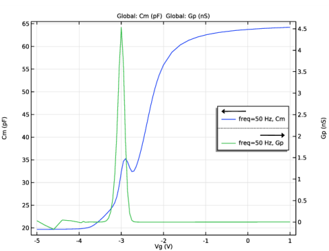
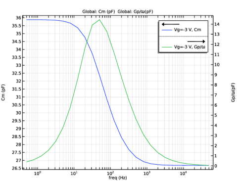
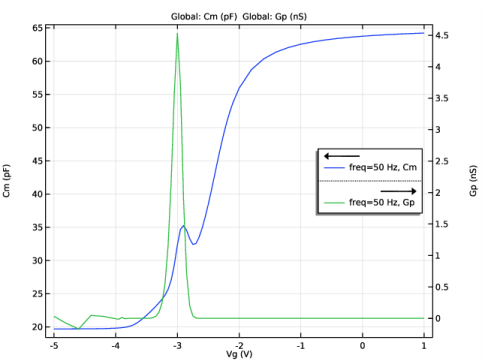
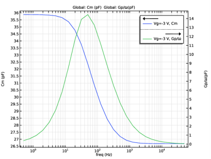
Locate the Data section. From the Dataset list, choose Study 2 - Freq sweep at -3 V/Solution 3 (sol3).
4
Locate the Legend section. From the Position list, choose Upper right.
Global 2
1
In the Model Builder window, expand the Cm and Gp vs. Freq node, then click Global 2.
2
In the Settings window for Global, locate the y-Axis Data section.
3
4
Locate the x-Axis Data section. From the Axis source data list, choose freq.
Global 1
1
In the Model Builder window, click Global 1.
2
In the Settings window for Global, locate the x-Axis Data section.
3
From the Axis source data list, choose freq.
4
Click the  x-Axis Log Scale button in the Graphics toolbar.
5
In the Cm and Gp vs. Freq toolbar, click  Plot.
To gain some insight on the behavior of the capacitance and conductance shown in the plots above, it helps to plot the trap occupancy along the energy axis. The energy axis is added to the model by the physics interface using an extra dimension component. To plot any quantity along the energy axis, we need to create a dataset pointing to the extra dimension component where the quantity is defined. We will first plot the density of states of the traps as an example.
Study 1 - Vg sweep at 50 Hz/Solution 1 XD
1
In the Model Builder window, expand the Results>Datasets node.
2
Right-click Results>Datasets>Study 1 - Vg sweep at 50 Hz/Solution 1 (sol1) and choose Duplicate.
3
In the Settings window for Solution, type Study 1 - Vg sweep at 50 Hz/Solution 1 XD in the Label text field.
4
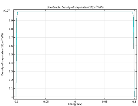
Locate the Solution section. From the Component list, choose Extra Dimension from Continuous Energy Levels 1 (semi_tasr1_ctb1_xdim).
Density of trap states vs. Energy
1
In the Home toolbar, click  Add Plot Group and choose 1D Plot Group.
2
In the Settings window for 1D Plot Group, type Density of trap states vs. Energy in the Label text field.
3
Locate the Data section. From the Dataset list, choose Study 1 - Vg sweep at 50 Hz/Solution 1 XD (sol1).
Line Graph 1
1
Right-click Density of trap states vs. Energy and choose Line Graph.
2
In the Settings window for Line Graph, locate the Selection section.
3
From the Selection list, choose All domains.
4
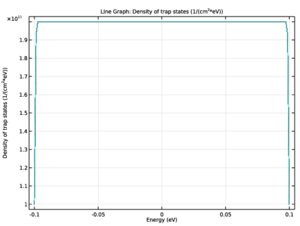
Locate the y-Axis Data section. In the Expression text field, type atxd0(0[um],(semi.tasr1.ctb1.gt/(e_const*Ew0))).
5
In the Unit field, type 1/(cm^2*eV).
6
Select the Description check box.
7
8
From the Expression evaluated for list, choose Static solution.
9
Locate the x-Axis Data section. From the Parameter list, choose Expression.
10
In the Expression text field, type atxd0(0[um],semi.tasr1.ctb1.Vxd-semi.tasr1.ctb1.Et0)*e_const.
11
From the Unit list, choose eV.
12
Select the Description check box.
13
14
From the Expression evaluated for list, choose Static solution.
15
In the Density of trap states vs. Energy toolbar, click  Plot.
Note that the operator atxd0 is used with a "0" because the energy axis (extra dimension) is defined in a boundary condition, which has a dimension of 0 in the 1D model. The first argument for the operator is 0[um] since the boundary condition is applied on the boundary located at 0 um. The x-axis for the energy is centered around the center of the trap energy level distribution. The density of trap states shows a rectangular distribution of 2e11[cm^-2*eV^-1] as specified. The option of Static solution is selected for both the x- and y-axes.
Now we plot the trap occupancy along the energy axis and compare two cases: gate voltage = 1 V (accumulation) and gate voltage = -3 V (peak of equilibrium parallel conductance). First the static solution.
Trap occupancy, static
1
In the Model Builder window, right-click Density of trap states vs. Energy and choose Duplicate.
2
In the Settings window for 1D Plot Group, type Trap occupancy, static in the Label text field.
3
Locate the Data section. From the Parameter selection (Vg) list, choose From list.
4
In the Parameter values (Vg (V)) list, choose 1 and -3.
5
Locate the Legend section. From the Position list, choose Lower left.
Line Graph 1
1
In the Model Builder window, expand the Trap occupancy, static node, then click Line Graph 1.
2
In the Settings window for Line Graph, locate the y-Axis Data section.
3
In the Expression text field, type atxd0(0[um],(semi.tasr1.ctb1.ft)).
4
In the Description text field, type Trap occupancy, static.
5
Click to expand the Legends section. Select the Show legends check box.
6
In the Trap occupancy, static toolbar, click  Plot.
The staircase like shape of the green curve is an indication of the 25 discrete levels used to approximate the continuous energy distribution as mentioned earlier. It is useful for developing purposes to be able to see these levels explicitly. Sometimes it is useful to smooth out the discretization for presentation purposes. This can be easily done by changing the Resolution option for the plot to No refinement.
7
Click to expand the Quality section. From the Resolution list, choose No refinement.
8
In the Trap occupancy, static toolbar, click  Plot.
We see that at the gate voltage of 1 V, since the Fermi level is far above the trap energy levels, the traps are fully occupied (blue curve). In this case one would not expect any significant contribution to the small signal response from the traps. On the other hand, at the gate voltage of -3 V, the Fermi level goes through the middle of the trap energy levels so that many trap levels are partially occupied (green curve). In this case one would expect the traps to contribute significantly to the small signal response, consistent with the peaking of the equivalent parallel conductance and the distinct wiggle of the measured capacitance curve seen in the earlier figure.
Finally, plot the small signal response of the trap occupancy along the energy axis and compare the same two cases: gate voltage = 1 V (accumulation) and gate voltage = -3 V (peak of equilibrium parallel conductance). Since the small signal response is complex valued, we plot both the real part (in solid curves) and the imaginary part (in dashed curves). Remember to select the Compute differential check box for the correct evaluation of the small signal response.
Trap occupancy, small signal response
1
In the Model Builder window, right-click Trap occupancy, static and choose Duplicate.
2
In the Model Builder window, click Trap occupancy, static 1.
3
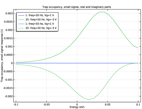
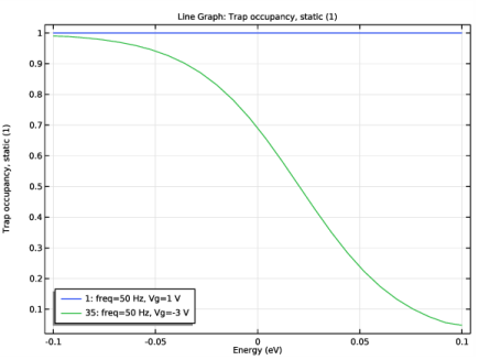
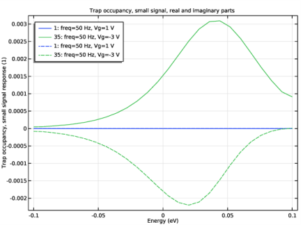
In the Settings window for 1D Plot Group, type Trap occupancy, small signal response in the Label text field.
4
Click to expand the Title section. From the Title type list, choose Manual.
5
In the Title text area, type Trap occupancy, small signal, real and imaginary parts.
6
Locate the Legend section. From the Position list, choose Upper left.
Line Graph 1
1
In the Model Builder window, click Line Graph 1.
2
In the Settings window for Line Graph, locate the y-Axis Data section.
3
In the Description text field, type Trap occupancy, small signal response.
4
From the Expression evaluated for list, choose Harmonic perturbation.
5
Select the Compute differential check box.
Line Graph 2
1
Right-click Results>Trap occupancy, small signal response>Line Graph 1 and choose Duplicate.
2
In the Settings window for Line Graph, locate the y-Axis Data section.
3
In the Expression text field, type atxd0(0[um],imag(semi.tasr1.ctb1.ft)).
4
Click to expand the Coloring and Style section. Find the Line style subsection. From the Line list, choose Dashed.
5
From the Color list, choose Cycle (reset).
6
In the Trap occupancy, small signal response toolbar, click  Plot.
We see that at the gate voltage of 1 V, both the real and imaginary parts of the small signal response of the trap occupancy are very small (blue curves). On the other hand, at the gate voltage of -3 V, both the real and imaginary parts of the small signal response of the trap occupancy are significant (green curves). All of these are consistent with the discussion above.