
|
|
|
|
|
|
1
|
|
2
|
|
3
|
Click Add.
|
|
4
|
Click
|
|
5
|
|
6
|
Click
|
|
1
|
|
2
|
|
1
|
|
2
|
|
1
|
|
2
|
|
4
|
|
5
|
|
6
|
|
1
|
|
2
|
|
3
|
|
5
|
|
6
|
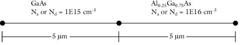
Browse to the model’s Application Libraries folder and double-click the file heterojunction_1d_gaas.txt.
|
|
1
|
|
2
|
|
3
|
|
5
|
|
6
|
Browse to the model’s Application Libraries folder and double-click the file heterojunction_1d_algaas.txt.
|
|
7
|
|
8
|
In the Show More Options dialog box, in the tree, select the check box for the node Physics>Advanced Physics Options.
|
|
9
|
Click OK.
|
|
1
|
|
2
|
|
3
|
|
1
|
In the Model Builder window, under Component 1 (comp1)>Semiconductor (semi) click Semiconductor Material Model 1.
|
|
2
|
|
3
|
|
1
|
|
2
|
|
3
|
|
1
|
|
3
|
|
4
|
|
1
|
|
1
|
|
2
|
|
4
|
|
5
|
|
1
|
|
2
|
In the Settings window for Analytic Doping Model, type Donor doping (right) in the Label text field.
|
|
4
|
|
5
|
|
1
|
|
2
|
In the Settings window for Analytic Doping Model, type Acceptor doping (left) in the Label text field.
|
|
4
|
|
1
|
|
2
|
In the Settings window for Analytic Doping Model, type Acceptor doping (right) in the Label text field.
|
|
4
|
|
1
|
|
3
|
|
4
|
|
1
|
In the Model Builder window, under Component 1 (comp1) right-click Materials and choose Blank Material.
|
|
2
|
|
1
|
|
2
|
|
3
|
|
4
|
|
5
|
|
6
|
|
7
|
|
1
|
|
2
|
|
3
|
|
1
|
|
2
|
|
3
|
|
4
|
In the Physics and variables selection tree, select Component 1 (comp1)>Semiconductor (semi)>Acceptor doping (left).
|
|
5
|
Click
|
|
6
|
In the Physics and variables selection tree, select Component 1 (comp1)>Semiconductor (semi)>Acceptor doping (right).
|
|
7
|
Click
|
|
8
|
In the Physics and variables selection tree, select Component 1 (comp1)>Semiconductor (semi)>Continuity/Heterojunction 2.
|
|
9
|
Click
|
|
10
|
|
11
|
|
12
|
Click
|
|
14
|
Click
|
|
16
|
|
1
|
|
2
|
|
3
|
|
4
|
|
5
|
In the Model Builder window, expand the n-n : Continuous Quasi-Fermi Levels>Solver Configurations>Solution 1 (sol1)>Dependent Variables 1 node, then click Electron solution variable (comp1.Ne).
|
|
6
|
|
7
|
|
8
|
|
9
|
|
10
|
|
11
|
|
12
|
|
13
|
|
14
|
|
15
|
|
16
|
Click
|
|
1
|
|
2
|
|
3
|
|
4
|
|
5
|
|
1
|
|
2
|
|
3
|
|
1
|
|
2
|
|
3
|
|
4
|
In the Physics and variables selection tree, select Component 1 (comp1)>Semiconductor (semi)>Acceptor doping (left).
|
|
5
|
Click
|
|
6
|
In the Physics and variables selection tree, select Component 1 (comp1)>Semiconductor (semi)>Acceptor doping (right).
|
|
7
|
Click
|
|
8
|
Click to expand the Values of Dependent Variables section. Find the Initial values of variables solved for subsection. From the Settings list, choose User controlled.
|
|
9
|
|
10
|
|
11
|
|
12
|
|
13
|
|
14
|
Click
|
|
16
|
Click
|
|
18
|
|
1
|
|
2
|
|
3
|
|
4
|
|
5
|
Click
|
|
1
|
|
2
|
|
3
|
|
4
|
|
5
|
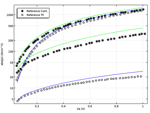
Browse to the model’s Application Libraries folder and double-click the file heterojunction_1d_case1_cont.txt.
|
|
1
|
|
2
|
|
3
|
|
4
|
Browse to the model’s Application Libraries folder and double-click the file heterojunction_1d_case1_te.txt.
|
|
1
|
|
2
|
|
3
|
|
4
|
|
5
|
|
6
|
|
7
|
|
8
|
In the associated text field, type abs(Jx) (A/cm^2).
|
|
9
|
|
1
|
|
2
|
|
3
|
|
4
|
|
5
|
|
6
|
|
7
|
|
8
|
|
10
|
|
1
|
|
2
|
|
3
|
|
4
|
Locate the Coloring and Style section. Find the Line markers subsection. From the Marker list, choose Circle.
|
|
5
|
Locate the Legends section. In the table, enter the following settings:
|
|
1
|
|
2
|
|
3
|
|
5
|
|
6
|
|
7
|
|
1
|
|
2
|
|
3
|
|
4
|
|
1
|
|
2
|
|
1
|
|
2
|
|
3
|
Find the Studies subsection. In the Select Study tree, select Preset Studies for Selected Physics Interfaces>Semiconductor Equilibrium.
|
|
4
|
|
5
|
|
1
|
In the Settings window for Semiconductor Equilibrium, locate the Physics and Variables Selection section.
|
|
2
|
|
3
|
In the Physics and variables selection tree, select Component 1 (comp1)>Semiconductor (semi)>Donor doping (left).
|
|
4
|
Click
|
|
5
|
In the Physics and variables selection tree, select Component 1 (comp1)>Semiconductor (semi)>Acceptor doping (right).
|
|
6
|
Click
|
|
7
|
|
8
|
|
9
|
|
1
|
|
2
|
|
3
|
|
4
|
In the Physics and variables selection tree, select Component 1 (comp1)>Semiconductor (semi)>Donor doping (left).
|
|
5
|
Click
|
|
6
|
In the Physics and variables selection tree, select Component 1 (comp1)>Semiconductor (semi)>Acceptor doping (right).
|
|
7
|
Click
|
|
8
|
|
9
|
|
10
|
Click
|
|
12
|
Click
|
|
1
|
|
2
|
|
3
|
|
4
|
|
5
|
Click
|
|
1
|
|
2
|
|
3
|
|
4
|
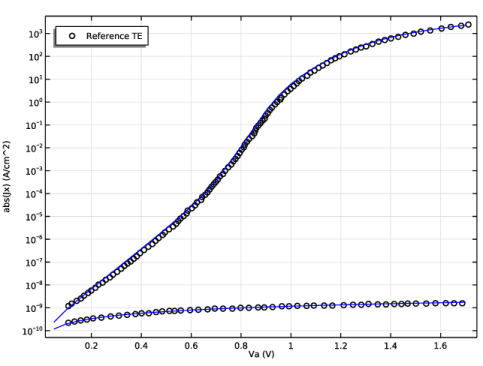
Browse to the model’s Application Libraries folder and double-click the file heterojunction_1d_case2_te.txt.
|
|
1
|
|
2
|
|
3
|
|
4
|
|
5
|
|
6
|
|
7
|
In the associated text field, type abs(Jx) (A/cm^2).
|
|
8
|
|
1
|
|
2
|
|
3
|
|
4
|
Locate the Coloring and Style section. Find the Line style subsection. From the Line list, choose None.
|
|
5
|
|
6
|
|
7
|
|
8
|
|
9
|
|
11
|
|
1
|
|
2
|
|
3
|
|
5
|
|
6
|
|
7
|
|
1
|
|
2
|
|
1
|
|
2
|
|
3
|
|
4
|
From the Doping and trap density continuation parameter list, choose Use interface continuation parameter.
|
|
1
|
In the Model Builder window, under Component 1 (comp1)>Semiconductor (semi) click Continuity/Heterojunction 2.
|
|
2
|
In the Settings window for Continuity/Heterojunction, click to expand the Continuation Settings section.
|
|
3
|
|
1
|
|
2
|
|
3
|
|
4
|
|
5
|
|
1
|
|
2
|
|
3
|
|
1
|
|
2
|
|
3
|
|
4
|
In the Physics and variables selection tree, select Component 1 (comp1)>Semiconductor (semi)>Donor doping (right).
|
|
5
|
Click
|
|
6
|
In the Physics and variables selection tree, select Component 1 (comp1)>Semiconductor (semi)>Acceptor doping (left).
|
|
7
|
Click
|
|
8
|
|
9
|
Click
|
|
1
|
|
2
|
|
3
|
|
4
|
In the Physics and variables selection tree, select Component 1 (comp1)>Semiconductor (semi)>Donor doping (right).
|
|
5
|
Click
|
|
6
|
In the Physics and variables selection tree, select Component 1 (comp1)>Semiconductor (semi)>Acceptor doping (left).
|
|
7
|
Click
|
|
8
|
|
9
|
|
10
|
Click
|
|
12
|
Click
|
|
14
|
|
1
|
|
2
|
|
3
|
|
4
|
|
5
|
Click
|
|
1
|
|
2
|
|
3
|
|
4
|
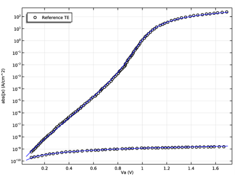
Browse to the model’s Application Libraries folder and double-click the file heterojunction_1d_case3_te.txt.
|
|
1
|
|
2
|
|
3
|
|
4
|
|
5
|
|
6
|
|
7
|
In the associated text field, type abs(Jx) (A/cm^2).
|
|
8
|
|
1
|
|
2
|
|
3
|
|
4
|
Locate the Coloring and Style section. Find the Line style subsection. From the Line list, choose None.
|
|
5
|
|
6
|
|
7
|
|
8
|
|
9
|
|
11
|
|
1
|
|
2
|
|
3
|
|
5
|
|
6
|
|
7
|
|
1
|
|
2
|
|
1
|
|
2
|
|
3
|
|
4
|
|
5
|
|
6
|
|
7
|
|
1
|
|
2
|
|
3
|
|
4
|
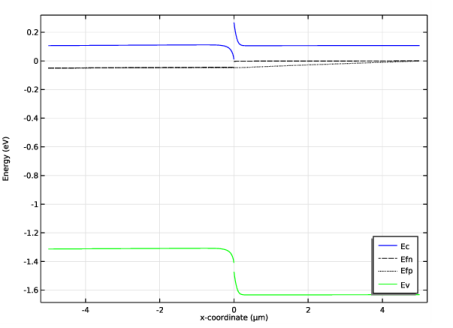
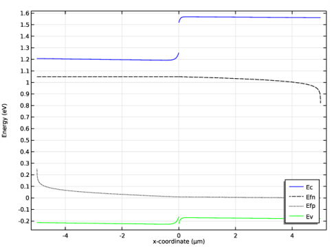
Click Replace Expression in the upper-right corner of the y-Axis Data section. From the menu, choose Component 1 (comp1)>Semiconductor>Fermi levels and band edges>Energies>semi.Ec_e - Conduction band energy level - J.
|
|
5
|
|
6
|
|
7
|
|
8
|
|
9
|
|
10
|
|
1
|
|
2
|
In the Settings window for Line Graph, click Replace Expression in the upper-right corner of the y-Axis Data section. From the menu, choose Component 1 (comp1)>Semiconductor>Fermi levels and band edges>Energies>semi.Efn_e - Electron quasi-Fermi energy level - J.
|
|
3
|
Locate the Coloring and Style section. Find the Line style subsection. From the Line list, choose Dashed.
|
|
4
|
|
5
|
Locate the Legends section. In the table, enter the following settings:
|
|
1
|
|
2
|
In the Settings window for Line Graph, click Replace Expression in the upper-right corner of the y-Axis Data section. From the menu, choose Component 1 (comp1)>Semiconductor>Fermi levels and band edges>Energies>semi.Efp_e - Hole quasi-Fermi energy level - J.
|
|
3
|
Locate the Coloring and Style section. Find the Line style subsection. From the Line list, choose Dotted.
|
|
4
|
Locate the Legends section. In the table, enter the following settings:
|
|
1
|
|
2
|
In the Settings window for Line Graph, click Replace Expression in the upper-right corner of the y-Axis Data section. From the menu, choose Component 1 (comp1)>Semiconductor>Fermi levels and band edges>Energies>semi.Ev_e - Valence band energy level - J.
|
|
3
|
Locate the Coloring and Style section. Find the Line style subsection. From the Line list, choose Solid.
|
|
4
|
|
5
|
Locate the Legends section. In the table, enter the following settings:
|
|
1
|
|
2
|
|
3
|
|
4
|
In the associated text field, type Energy (eV).
|
|
5
|
|
6
|
|
1
|
|
2
|
|
3
|
|
4
|
|
5
|
|
6
|
|
1
|
|
2
|
|
3
|
|
4
|