PDF

InGaN/AlGaN Double Heterostructure LED
This model simulates a GaN-based light emitting diode (LED). It demonstrates how the Semiconductor interface can be used to evaluate optical emission from electrically driven optoelectronic devices using the Optical Transition feature. It also gives an example of how current-driven problems can be solved by first generating suitable initial conditions from voltage-driven studies. The emission spectrum, intensity, and quantum efficiency are calculated as a function of the driving current in order to evaluate the optimum operating conditions. Note that quantum confinement effects within the thin active region are not included in the model.
Introduction
LEDs are revolutionizing the lighting industry, as they are often much more efficient and durable than traditional incandescent light technologies. For example, typical consumer LED light bulbs operate at 10–20% of the power needed to run an incandescent bulb of comparable brightness and have lifetimes of over 25,000 hours, compared to only 1000 hours for incandescent bulbs. LEDs are so much more efficient than incandescent bulbs because they function in a very different way. LEDs are semiconductor devices that emit light when electrons in the conduction band transition across the band gap via radiative recombination with holes in the valence band. Incandescent bulbs rely on resistive heating of a filament, which emits light when it has become hot enough to glow. This uses lots of energy just to heat the filament, and only a smaller fraction of output energy goes into light production. The high temperatures involved also lead to shorter lifetimes, as burnt out filaments are nearly always the cause of incandescent bulb failures.
Unlike incandescent bulbs, LEDs emit light over a very narrow range of wavelengths. Initially, red, green, and yellow LEDs were developed in the 1950s–1960s; however, it was the invention of the blue LED that led to the creation of new efficient white light sources. Blue light emitted from such LEDs can be used to stimulate a wider spectrum of emission from a phosphor layer around the LED casing or can be directly combined with red and green LEDs to create white light.
The blue LEDs were more challenging to develop in part because they require a larger band-gap material. The first high efficiency blue LED was created in 1994, and the 2014 Noble Prize in Physics was awarded to Isamu Akasaki, Hiroshi Amano, and Shuji Nakamura for their work toward this achievement. A summary of the history of LED development can be found in Ref. 1.
Although LEDs are much more efficient than previous lighting technology, there are still some science and engineering challenges to overcome to further improve their design. In particular, the efficiency of LEDs decreases at larger driving currents. This phenomenon is known as LED droop and causes the total emitted light to increase sublinearly with increased current bias, restricting the intensity that can be achieved whilst maintaining high efficiency. Consequently, to increase the total brightness it is often necessary to increase the area of the device, or add additional LEDs to a bulb, rather than simply applying more current. This adds to the expense of the bulb and increases the cost of LED products.
In this model, the active light-emitting region of a GaN-based blue LED is modeled. The emission properties are investigated as a function of driving current, and the efficiency is calculated.
Model Definition
The materials and geometry of this model are based on the device described by Nakamura et al. in Ref. 2. Only the active double heterojunction region, from which the desired wavelength of light is emitted, is modeled. This region consists of a 50 nm thick layer of In0.06Ga0.94N, sandwiched between 0.15 μm thick layers of Al0.15Ga0.85N. As the device is laterally invariant, it can be modeled using a 1D line cut in the z direction, as shown in Figure 1. The cross sectional area of the device is calculated assuming the active region has lateral dimensions of 200-by-200 μm, which is a typical LED mesa size.
The lower AlGaN layer is n-doped and the upper AlGaN layer is p-doped. The InGaN layer is undoped. This creates a PIN diode structure, with the light emitting InGaN layer in the central intrinsic (undoped) region. The material properties are based on the GaN material from the semiconductor module material library. However, the band-gap energy and electron affinity values have been changed to reflect the In and Al alloy compositions. Note that the band gap of the InGaN material has been selected to match the spectral range of the emission from the device in Ref. 2. As well as amending these properties, Auger recombination factors and carrier lifetimes for Trap-Assisted recombination have been added to the materials. Values for these properties were found in Ref. 3 and Ref. 4. Note that quantum confinement effect are not included in this model.
Although the polarization charge effect is not included in this model, it is straightforward to add it by first computing the surface and/or space charge densities from the polarization field, then enter them into the Surface Charge Density boundary condition and/or the Space Charge Density domain condition.
Figure 1: Geometry and doping of the LED device. Left: Structure of the LED on which this model is based. The section which is modeled is highlighted with a red bar. Top right: The geometry models the double heterostructure region of the full device. Lower-right: The doping profile is a PIN diode with the InGaN layer forming the intrinsic region.
Metal contact boundary conditions are applied to the bounds of the geometry in order to apply voltage and current biases to the device. In addition, a second Continuity/Heterojunction boundary condition is added to enable toggling between the continuous quasi-Fermi levels and thermionic emission heterojunction continuity models. An Optical Transitions feature is used to calculate the spontaneous emission from the device. Non-radiative recombination mechanisms are included via Auger Recombination and Trap-Assisted Recombination features, which are added to all domains.
Three studies are used to solve the current driven model. The first study is a preliminary study, which uses the Semiconductor Equilibrium study step to obtain the equilibrium solution as the initial condition for the following study.
The equation system for heterojunctions is highly nonlinear and numerically challenging. In this tutorial we uses the Semiconductor Equilibrium study step to achieve better convergence. See the verification model example heterojunction_1d for more ways to overcome the numerical challenge.
The second study is a voltage biased study, which sweeps the applied voltage across the device from 0 to 3.3 V. From this study, the energy level diagram for the device is created, along with the carrier concentration distribution and a current-voltage curve.
The final study is a current biased study, which sweeps the applied current driven through the device over several orders of magnitude from 1 μA to 700 mA. This study uses a solution from the voltage driven study as the initial conditions in order to converge. The data from this study is added to the current-voltage curve to ensure agreement with the voltage driven case. The emission rate throughout the device, emission spectrum from the InGaN material, total emission rate integrated over the InGaN layer, and internal quantum efficiency, are then plotted as a function of the current bias.
Results and Discussion
The energy level diagram for the device is shown at two different voltage biases in Figure 2 and Figure 3. The conduction and valence band are labeled semi.Ec and semi.Ev, respectively, and the electron and hole quasi-Fermi levels are labeled semi.Efn and semi.Efp, respectively. In both cases the PIN doping is apparent, as it causes a potential barrier between the left hand n-doped region and the right hand p-doped region. The lower band gap InGaN layer causes a potential well in both the conduction and valence bands. For a fully accurate simulation quantum confinement effects of this 50 nm thick well should be accounted for. These effects are not included in this model. The main consequence of this is that the calculated emission spectrum will not include contributions from bound exciton states or transitions between quantum confined energy levels in the two potential wells. In the zero bias case (Figure 2) the quasi-Fermi levels are far from the band edges in the InGaN layer. This is expected when the device is in equilibrium and no light is being emitted. When a voltage of 3.3 V is applied to the p-side of the device (Figure 3) the forward bias has reduced the height of the potential barrier between the n-type and p-type regions as expected. The electron quasi-Fermi energy level is now above the conduction band edge in the InGaN layer, so we expect the conduction band to be populated with electrons in this region. The hole quasi-Fermi energy level is very close to the valence band edge, so we expect the valence band to be populated with holes.
Figure 2: Energy level diagram for the case of zero bias. The conduction band (semi.Ec) and valence band (semi.Ev) show a potential barrier between the left hand n-doped and right hand p-doped regions. The InGaN layer creates a potential well in both bands.
Figure 3: Energy level diagram for a forward voltage bias of 3.3 V. The height of the potential barrier has been reduced by the forward bias.
.
Figure 4: Carrier concentration at zero bias. The n-type and p-type regions have large concentrations of electron and holes, respectively. The depleted region has a small increase in carrier concentration in the InGaN layer due to the potential well, however the concentration is orders of magnitude smaller than the surrounding material.
Figure 5: Carrier concentration at a 3.3 V forward bias. The InGaN layer is heavily populated with both electrons in the conduction band and holes in the valence band.
Figure 4 and Figure 5 show the carrier concentration throughout the device at zero and 3.3 V forward bias, respectively. As expected, the InGaN region is not populated with carriers in the equilibrium case, but the application of a forward bias causes carriers to collect in the potential well created by the InGaN layer. Importantly, the concentration of electrons in the conduction band is of similar magnitude to the concentration of holes in the valence band. This allows for efficient light output, as each photon that is emitted requires an electron to recombine across the band gap with a hole.
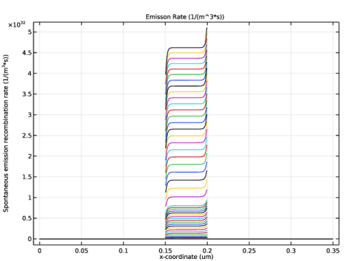
Figure 6 shows the emission rate throughout the device for the range of current biases. In all cases the emission from the InGaN layer is significantly larger than in the cladding material. This is because the InGaN layer is the only region of the device which has a high concentration of both electrons and holes. As the current bias increases so does the rate of emission, due to the increased carrier injection rate.
Figure 6: Emission rate throughout the device for a range of current biases. The emission rate is largest in the InGaN layer, as this region has a plentiful supply of both electrons in the conduction band and holes in the valence band.
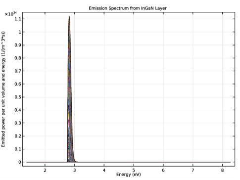
The emission spectrum from the center of the InGaN layer is shown in Figure 7. The peak emission occurs around photon energies of 2.8–2.9 eV, which corresponds to a wavelength range of ~430–445 nm. This falls inside the target blue range of the spectrum, as expected since the band gap for the InGaN layer was calculated to match the emission spectrum from the device described in Ref. 2. Again it is clear that with increased current the total emission intensity increases.
Figure 7: Emission spectrum from the center of the InGaN layer.
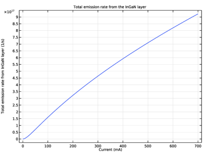
Although the total light emitted increases with current bias, it is not always favorable to simply operate at larger currents to increase the device brightness. This is because the efficiency of the device decreases with increased current density, resulting in a sublinear increase in the total emission rate with current bias. Figure 8 shows the total emission rate from the InGaN layer as a function of the applied current bias, and this effect is clearly visible. This phenomenon is known as LED droop, and is a subject of ongoing research within the solid-state lighting community. One metric by which the efficiency can be assessed is the Internal Quantum Efficiency (IQE). This is the fraction of injected carriers that radiatively recombine in the InGaN layer. Figure 9 shows the IQE as a function of the current density. There is a peak in the IQE at current densities around 30 A cm-2 and for densities in excess of ~100 A cm-2 there is a rapid drop off in the IQE. The peak efficiency is achieved with applied currents in the 10–30 mA range, which is typical for LED devices of this size.
Figure 8: Total emission rate from the InGaN layer as a function of current bias. The sublinear increase is characteristic of LED droop and is common to LED devices.
Figure 9: Internal Quantum Efficiency as a function of current density. The rapid decrease for densities above ~100 A cm-2 limits the current bias which can be applied whilst maintaining acceptable efficiency.
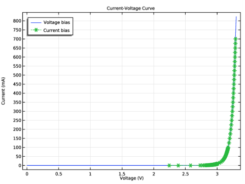
The current-voltage curve in Figure 10 highlights the significance of the LED droop problem. The optimum efficiency occurs at currents which are only slightly above the turn-on threshold. The device could function at much larger currents without any electrical issues, however the drop in IQE limits the current to a small fraction of its potential maximum value if high efficiency is desired.
Figure 10: The current-voltage curve for the device under both voltage and current bias. The two studies are in agreement. The optimum efficiency is achieved with currents in the 10-30 mA range, which occur at voltage slightly above the turn-on threshold.
The cause of LED droop is yet to be fully understood. In this model, the drop in IQE is due to the nonradiative recombination mechanisms which are included. The rate of Auger recombination is proportional to the cube of the carrier density, whilst the rate of direct radiative recombination is proportional to only the square of the carrier density. This causes the fraction of recombination events which occur via the radiative mechanism to greatly reduce as the carrier density is increased. Hence the drop in efficiency for increased current densities.
References
1. The Nobel Prize in Physics 2014 - Advanced Information. Nobelprize.org., Nobel Media AB 2014. Web. 29 Oct 2014. http://www.nobelprize.org/nobel_prizes/physics/laureates/2014/advanced.html
2. S. Nakamura,T. Mukia, and M. Senoh, “Candelaclass highbrightness InGaN/AlGaN doubleheterostructure bluelight emitting diodes,” Appl. Phys. Lett., vol. 64, p. 1687, 1994.
3. Y.C. Shen, G.O. Mueller, S. Watanabe, N.F. Gardner, A. Munkholm, and M.R. Krames, Auger recombination in InGaN measured by photoluminescence,” Appl. Phys. Lett., vol. 91, p. 141101, 2007.
4. Q. Dai and others, “Internal quantum efficiency and nonradiative recombination coefficient of GaInN/GaN multiple quantum wells with different dislocation densities,” Appl. Phys. Lett., vol. 94, p. 111109, 2009.
Application Library path: Semiconductor_Module/Photonic_Devices_and_Sensors/gan_double_heterostructure_led
Modeling Instructions
From the File menu, choose New.
New
In the New window, click  Model Wizard.
Model Wizard
1
In the Model Wizard window, click  1D.
2
In the Select Physics tree, select Semiconductor>Semiconductor (semi).
3
Click Add.
The first study will be a preliminary study that is used to create initial conditions for the subsequent voltage biased study. This is needed due to the nonlinear nature of the equations involved in modeling recombination effects and heterojunctions.
There are several different ways to overcome the numerical challenge posted by the nonlinearity in the equation system. Here we use the Semiconductor Equilibrium study step to obtain the equilibrium solution as the initial condition for the following study. For other alternative ways to achieve convergence, see the verification model example heterojunction_1d.
4
Click  Study.
5
In the Select Study tree, select Preset Studies for Selected Physics Interfaces>Semiconductor Equilibrium.
6
Add some global parameters to the model.
Global Definitions
Parameters 1
1
In the Model Builder window, under Global Definitions click Parameters 1.
2
In the Settings window for Parameters, locate the Parameters section.
3
Create the model geometry.
Geometry 1
1
In the Model Builder window, under Component 1 (comp1) click Geometry 1.
2
In the Settings window for Geometry, locate the Units section.
3
From the Length unit list, choose µm.
Interval 1 (i1)
1
Right-click Component 1 (comp1)>Geometry 1 and choose Interval.
2
In the Settings window for Interval, locate the Interval section.
3
Interval 2 (i2)
1
In the Model Builder window, right-click Geometry 1 and choose Interval.
2
In the Settings window for Interval, locate the Interval section.
3
Interval 3 (i3)
1
Right-click Geometry 1 and choose Interval.
2
In the Settings window for Interval, locate the Interval section.
3
Add materials to the geometry domains. The two cladding layers are Al0.15Ga0.85N, which has a band gap energy of 3.7 eV. The central layer is In0.06Ga0.94N. The band gap energy of the InGaN has been estimated from the emission spectra in the reference paper. The electron affinity of the InGaN has been set such that the central layer creates a potential well for both electrons in the conduction band and holes in the valence band.
Add Material
1
In the Home toolbar, click  Add Material to open the Add Material window.
2
Go to the Add Material window.
3
In the tree, select Semiconductors>GaN (Zinc Blende) - Gallium Nitride.
4
Click Add to Component in the window toolbar.
5
Click Add to Component in the window toolbar.
Materials
Al_0.15_Ga_0.85_N
1
In the Settings window for Material, type Al_0.15_Ga_0.85_N in the Label text field.
2
Locate the Material Contents section. In the table, enter the following settings:
In_0.06_Ga_0.94_N
1
In the Model Builder window, under Component 1 (comp1)>Materials click GaN (Zinc Blende) - Gallium Nitride 1 (mat2).
2
In the Settings window for Material, type In_0.06_Ga_0.94_N in the Label text field.
3
Locate the Geometric Entity Selection section. Click  Paste Selection.
4
In the Paste Selection dialog box, type 2 in the Selection text field.
5
6
In the Settings window for Material, locate the Material Contents section.
7
8
In the Home toolbar, click  Add Material to close the Add Material window.
Create a nonlocal integration coupling in the component definitions node. This will allow the emission rate to be integrated over the entire InGaN layer when creating graphs later.
Definitions
Integration 1 (intop1)
1
In the Definitions toolbar, click  Nonlocal Couplings and choose Integration.
2
In the Settings window for Integration, locate the Source Selection section.
3
Click  Paste Selection.
4
In the Paste Selection dialog box, type 2 in the Selection text field.
5
Next configure the physics in the Semiconductor interface.
Semiconductor (semi)
1
In the Model Builder window, under Component 1 (comp1) click Semiconductor (semi).
2
In the Settings window for Semiconductor, locate the Cross-Section Area section.
3
In the A text field, type A_cross.
4
Locate the Model Properties section. From the Carrier statistics list, choose Fermi-Dirac.
n Doping
1
In the Physics toolbar, click  Domains and choose Analytic Doping Model.
2
In the Settings window for Analytic Doping Model, type n Doping in the Label text field.
3
Locate the Domain Selection section. From the Selection list, choose All domains.
4
Locate the Distribution section. From the list, choose Box.
5
Locate the Impurity section. From the Impurity type list, choose Donor doping (n-type).
6
In the ND0 text field, type 1e18[1/cm^3].
7
Locate the Uniform Region section. In the W text field, type 0.125[um].
8
Locate the Profile section. In the dj text field, type 0.025[um].
p Doping
1
In the Physics toolbar, click  Domains and choose Analytic Doping Model.
2
In the Settings window for Analytic Doping Model, type p Doping in the Label text field.
3
Locate the Domain Selection section. From the Selection list, choose All domains.
4
Locate the Distribution section. From the list, choose Box.
5
Locate the Impurity section. In the NA0 text field, type 1e18[1/cm^3].
6
Locate the Uniform Region section. Specify the r0 vector as
7
In the W text field, type 0.125[um].
8
Locate the Profile section. In the dj text field, type 0.025[um].
n Contact
1
In the Physics toolbar, click  Boundaries and choose Metal Contact.
2
In the Settings window for Metal Contact, type n Contact in the Label text field.
3
4
Locate the Terminal section. In the V0 text field, type V_n.
p Contact
1
In the Physics toolbar, click  Boundaries and choose Metal Contact.
2
In the Settings window for Metal Contact, type p Contact in the Label text field.
3
4
Locate the Terminal section. In the V0 text field, type V_p.
Continuity/Heterojunction - Thermionic Emission
1
In the Physics toolbar, click  Boundaries and choose Continuity/Heterojunction.
2
In the Settings window for Continuity/Heterojunction, locate the Boundary Selection section.
3
From the Selection list, choose All boundaries.
4
In the Label text field, type Continuity/Heterojunction - Thermionic Emission.
5
Locate the Heterojunction section. From the Continuity model list, choose Thermionic emission.
Optical Transitions 1
1
In the Physics toolbar, click  Domains and choose Optical Transitions.
2
In the Settings window for Optical Transitions, locate the Domain Selection section.
3
From the Selection list, choose All domains.
4
Locate the Optical Transitions section. Clear the Stimulated absorption and emission check box.
p Contact - Current
1
In the Physics toolbar, click  Boundaries and choose Metal Contact.
2
In the Settings window for Metal Contact, type p Contact - Current in the Label text field.
3
4
Locate the Terminal section. From the Terminal type list, choose Current.
5
In the I0 text field, type I_p.
Auger Recombination 1
1
In the Physics toolbar, click  Domains and choose Auger Recombination.
2
In the Settings window for Auger Recombination, locate the Domain Selection section.
3
From the Selection list, choose All domains.
Trap-Assisted Recombination 1
1
In the Physics toolbar, click  Domains and choose Trap-Assisted Recombination.
2
In the Settings window for Trap-Assisted Recombination, locate the Domain Selection section.
3
From the Selection list, choose All domains.
The two nonradiative recombination mechanisms require extra material properties to be added. Auger recombination factors and Shockley-Read-Hall (SHR) carrier lifetimes have been looked up in recent literature, however these parameters are highly dependent on the material growth conditions so there is a rather wide range of plausible values.
Materials
Al_0.15_Ga_0.85_N (mat1)
1
In the Model Builder window, under Component 1 (comp1)>Materials click Al_0.15_Ga_0.85_N (mat1).
2
In the Settings window for Material, locate the Material Contents section.
3
In_0.06_Ga_0.94_N (mat2)
1
In the Model Builder window, click In_0.06_Ga_0.94_N (mat2).
2
In the Settings window for Material, locate the Material Contents section.
3
Configure a suitable mesh.
Mesh 1
Edge 1
1
In the Mesh toolbar, click  Edge.
2
In the Settings window for Edge, locate the Domain Selection section.
3
From the Geometric entity level list, choose Entire geometry.
Distribution 1
1
Right-click Edge 1 and choose Distribution.
2
3
In the Settings window for Distribution, locate the Distribution section.
4
From the Distribution type list, choose Predefined.
5
In the Number of elements text field, type 100.
6
In the Element ratio text field, type 6.
7
Select the Symmetric distribution check box.
Distribution 2
1
In the Model Builder window, right-click Edge 1 and choose Distribution.
2
3
In the Settings window for Distribution, locate the Distribution section.
4
From the Distribution type list, choose Predefined.
5
In the Number of elements text field, type 30.
6
In the Element ratio text field, type 2.
7
Select the Symmetric distribution check box.
8
Click  Build All.
Configure the first study, which is a preliminary study that is used to create initial conditions for the subsequent voltage biased study. This is needed due to the nonlinear nature of the equations involved in modeling recombination effects and heterojunctions.
There are several different ways to overcome the numerical challenge posted by the nonlinearity in the equation system. Here we use the Semiconductor Equilibrium study step to obtain the equilibrium solution as the initial condition for the following study. For other alternative ways to achieve convergence, see the verification model example heterojunction_1d.
Study 1: Preliminary study
1
In the Model Builder window, click Study 1.
2
In the Settings window for Study, type Study 1: Preliminary study in the Label text field.
3
Locate the Study Settings section. Clear the Generate default plots check box.
4
In the Home toolbar, click  Compute.
Next configure the second study to perform a voltage bias sweep. The voltage across the device will be varied from 0 to 3.5 V by sweeping the value of the parameter V_p. The solution from the preliminary study is used for the initial values of the dependent variables.
Add Study
1
In the Home toolbar, click  Add Study to open the Add Study window.
2
Go to the Add Study window.
3
Find the Studies subsection. In the Select Study tree, select General Studies>Stationary.
4
Click Add Study in the window toolbar.
5
In the Home toolbar, click  Add Study to close the Add Study window.
Study 2: Voltage bias
1
In the Model Builder window, click Study 2.
2
In the Settings window for Study, type Study 2: Voltage bias in the Label text field.
Step 1: Stationary
1
In the Model Builder window, under Study 2: Voltage bias click Step 1: Stationary.
2
In the Settings window for Stationary, locate the Physics and Variables Selection section.
3
Select the Modify model configuration for study step check box.
4
In the Physics and variables selection tree, select Component 1 (comp1)>Semiconductor (semi)>p Contact - Current.
5
Click  Disable.
6
Click to expand the Values of Dependent Variables section. Find the Initial values of variables solved for subsection. From the Settings list, choose User controlled.
7
From the Method list, choose Solution.
8
From the Study list, choose Study 1: Preliminary study, Semiconductor Equilibrium.
9
Click to expand the Study Extensions section. Select the Auxiliary sweep check box.
10
11
12
In the Home toolbar, click  Compute.
Results
Energy Levels (semi)
The default plot groups show the energy level diagram, carrier concentrations, and electric potential for the device. Plotting only the data at one bias voltage allows the results to be viewed with more clarity.
1
In the Settings window for 1D Plot Group, locate the Plot Settings section.
2
Select the x-axis label check box.
3
4
Locate the Data section. From the Parameter selection (V_p) list, choose From list.
5
In the Parameter values (V_p (V)) list, select 0.
6
In the Energy Levels (semi) toolbar, click  Plot.
The response of the energy levels as the bias is increased can be observed by varying the value of V_p for which the data is plotted. This is done by selecting values from the Parameter values (V_p) selection box.
7
In the Parameter values (V_p (V)) list, select 3.3.
8
In the Energy Levels (semi) toolbar, click  Plot.
As the forward bias is increased the height of the potential barrier between the n and p-type regions is reduced as the bands "flatten out". The quasi-Fermi levels also move closer to the band edges, reflecting the fact that more carriers are flowing through the device, leading to an increased probability that carriers are in the quantum well region formed by the lower band gap InGaN layer.
The Carrier Concentration plot shows that the population of carriers in the InGaN layer increases drastically with the increased bias. Again, this can be seen more clearly by selecting to plot data for one value of V_p at a time and switching through different values.
Carrier Concentrations (semi)
1
In the Model Builder window, click Carrier Concentrations (semi).
2
In the Settings window for 1D Plot Group, locate the Plot Settings section.
3
Select the x-axis label check box.
4
5
Locate the Data section. From the Parameter selection (V_p) list, choose From list.
6
In the Parameter values (V_p (V)) list, select 0.
7
In the Carrier Concentrations (semi) toolbar, click  Plot.
8
In the Parameter values (V_p (V)) list, select 3.3.
9
In the Carrier Concentrations (semi) toolbar, click  Plot.
This is the expected behavior, as the bias is increased more current flows through the device and the carrier concentration in the InGaN layer is increased. Importantly, the concentration of both electrons and holes peaks in the InGaN layer, which causes the radiative recombination to be localized to this region. This will be seen when the rate of spontaneous emission throughout the devices is plotted after the next study.
The I-V curve for the device can be created by plotting the current as a function of the applied bias. This shows that the device displays typical diode behavior as expected.
Current vs. Voltage
1
In the Home toolbar, click  Add Plot Group and choose 1D Plot Group.
2
In the Settings window for 1D Plot Group, type Current vs. Voltage in the Label text field.
3
Locate the Data section. From the Dataset list, choose Study 2: Voltage bias/Solution 2 (sol2).
4
Click to expand the Title section. From the Title type list, choose Manual.
5
In the Title text area, type Current-Voltage Curve.
6
Locate the Plot Settings section. Select the x-axis label check box.
7
8
Select the y-axis label check box.
9
10
Locate the Legend section. From the Position list, choose Upper left.
Global 1
1
Right-click Current vs. Voltage and choose Global.
2
In the Settings window for Global, locate the y-Axis Data section.
3
4
In the Current vs. Voltage toolbar, click  Plot.
Next configure a final study to perform a current bias sweep. This study will use the p contact - current boundary condition to apply a range of currents to the device. It uses a solution from the previous voltage driven study as an initial condition. In order to find which value of V_p gives the best initial solution for the current bias study, a global evaluation can be used to view the current as a function of V_p from the Voltage bias study.
Global Evaluation 1
1
In the Results toolbar, click  Global Evaluation.
2
In the Settings window for Global Evaluation, locate the Data section.
3
From the Dataset list, choose Study 2: Voltage bias/Solution 2 (sol2).
4
Locate the Expressions section. In the table, enter the following settings:
5
Click  Evaluate.
The current bias study will begin with an applied bias of 1 uA, from the table we can see that this magnitude of current flows when a voltage of V_p=2.2 V is applied. Therefore we will choose the corresponding solution for the initial condition in the current bias study, and set the Initial voltage input field of the current-driven metal contact boundary condition to the same value. Note that the range of applied currents is chosen to resolve nonlinear features in the Current versus Voltage plot and a subsequent plot of the efficiency.
Semiconductor (semi)
p Contact - Current
1
In the Model Builder window, under Component 1 (comp1)>Semiconductor (semi) click p Contact - Current.
2
In the Settings window for Metal Contact, locate the Terminal section.
3
In the Vinit text field, type 2.2[V].
Add Study
1
In the Home toolbar, click  Add Study to open the Add Study window.
2
Go to the Add Study window.
3
Find the Studies subsection. In the Select Study tree, select General Studies>Stationary.
4
Click Add Study in the window toolbar.
5
In the Home toolbar, click  Add Study to close the Add Study window.
Study 3: Current bias
1
In the Model Builder window, click Study 3.
2
In the Settings window for Study, type Study 3: Current bias in the Label text field.
3
Locate the Study Settings section. Clear the Generate default plots check box.
Step 1: Stationary
1
In the Model Builder window, under Study 3: Current bias click Step 1: Stationary.
2
In the Settings window for Stationary, locate the Values of Dependent Variables section.
3
Find the Initial values of variables solved for subsection. From the Settings list, choose User controlled.
4
From the Method list, choose Solution.
5
From the Study list, choose Study 2: Voltage bias, Stationary.
6
From the Parameter value (V_p (V)) list, choose 2.2 V.
7
Locate the Study Extensions section. Select the Auxiliary sweep check box.
8
9
10
In the Home toolbar, click  Compute.
Add the data from the current driven study to the Current vs. Voltage plot group.
Results
Global 2
1
In the Model Builder window, under Results>Current vs. Voltage right-click Global 1 and choose Duplicate.
2
In the Settings window for Global, locate the Data section.
3
From the Dataset list, choose Study 3: Current bias/Solution 3 (sol3).
4
Locate the y-Axis Data section. In the table, enter the following settings:
5
Locate the x-Axis Data section. From the Parameter list, choose Expression.
6
In the Expression text field, type semi.V0_3.
7
Click to expand the Coloring and Style section. Find the Line style subsection. From the Line list, choose Dashed.
8
Find the Line markers subsection. From the Marker list, choose Cycle.
9
From the Positioning list, choose In data points.
10
In the Current vs. Voltage toolbar, click  Plot.
Plot the rate of radiative transitions throughout the device from the current bias dataset. Notice how the emission is concentrated in the active InGaN layer as expected, and that increasing the current increases the rate of emission.
Emission Rate
1
In the Home toolbar, click  Add Plot Group and choose 1D Plot Group.
2
In the Settings window for 1D Plot Group, type Emission Rate in the Label text field.
3
Locate the Data section. From the Dataset list, choose Study 3: Current bias/Solution 3 (sol3).
4
Locate the Title section. From the Title type list, choose Manual.
5
In the Title text area, type Emisson Rate (1/(m^3*s)).
6
Locate the Plot Settings section. Select the x-axis label check box.
7
Line Graph 1
1
Right-click Emission Rate and choose Line Graph.
2
In the Settings window for Line Graph, locate the Selection section.
3
From the Selection list, choose All domains.
4
Locate the y-Axis Data section. In the Expression text field, type semi.ot1.R_spon.
5
In the Emission Rate toolbar, click  Plot.
Create a solution dataset to hold the extra dimension data, which allows quantities to be plotted in the frequency domain. The emission spectrum from the InGaN layer can then be plotted.
Current bias study - frequency domain
1
In the Results toolbar, click  More Datasets and choose Solution.
2
In the Settings window for Solution, locate the Solution section.
3
From the Solution list, choose Solution 3 (sol3).
4
From the Component list, choose Extra Dimension from Optical Transitions 1 (semi_ot1_xdim).
5
In the Label text field, type Current bias study - frequency domain.
The emission spectrum can be plotted using the expression comp1.atxd1(0.1525e-6,semi.ot1.dP_dE). The variable semi.ot1.dP_dE is the emitted power per unit volume and energy. The command comp1.atxd1(coord,var) gets the variable var, which is calculated in an extra dimension attached to component 1, from coordinate coord in the model geometry.
In this case, coordinate 0.1525e-6 corresponds to the center of the InGaN layer, so this command gets semi.ot1.dP_dE as a function of frequency (the extra dimension) at this spatial point.
The default x-axis for the plot is a normalized variable which is proportional to the angular frequency, with x = 1 corresponding to the angular frequency of the band gap energy. In order to plot the data as a function of energy the expression hbar_const*comp1.atxd1(0.1525e-6,semi.ot1.omega)/e_const is used. The variable semi.ot1.omega returns the angular frequency, which is then converted into energy in eV via multiplication by hbar_const and division by e_const.
Emission Spectrum
1
In the Results toolbar, click  1D Plot Group.
2
In the Settings window for 1D Plot Group, type Emission Spectrum in the Label text field.
3
Locate the Data section. From the Dataset list, choose Current bias study - frequency domain (sol3).
4
Locate the Title section. From the Title type list, choose Manual.
5
In the Title text area, type Emission Spectrum from InGaN Layer.
6
Locate the Plot Settings section. Select the x-axis label check box.
7
8
Select the y-axis label check box.
9
In the associated text field, type Emitted power per unit volume and energy (1/(m^3*s)).
Line Graph 1
1
Right-click Emission Spectrum and choose Line Graph.
2
In the Settings window for Line Graph, locate the Selection section.
3
From the Selection list, choose All domains.
4
Locate the y-Axis Data section. In the Expression text field, type comp1.atxd1(0.1525e-6,semi.ot1.dP_dE).
5
Locate the x-Axis Data section. From the Parameter list, choose Expression.
6
In the Expression text field, type hbar_const*comp1.atxd1(0.1525e-6,semi.ot1.omega)/e_const.
7
In the Emission Spectrum toolbar, click  Plot.
From the emission rate and spectra it can be seen that as the current is increased the emission intensity of the LED increases. This can be seen more clearly by plotting the total emitted intensity integrated over the InGaN layer as a function of current bias.
Total Emission Rate from InGaN Layer vs. Current
1
In the Home toolbar, click  Add Plot Group and choose 1D Plot Group.
2
In the Settings window for 1D Plot Group, type Total Emission Rate from InGaN Layer vs. Current in the Label text field.
3
Locate the Data section. From the Dataset list, choose Study 3: Current bias/Solution 3 (sol3).
4
Locate the Plot Settings section. Select the x-axis label check box.
5
6
Select the y-axis label check box.
7
In the associated text field, type Total emission rate from InGaN layer (1/s).
8
Locate the Title section. From the Title type list, choose Manual.
9
In the Title text area, type Total emission rate from the InGaN layer.
Global 1
1
Right-click Total Emission Rate from InGaN Layer vs. Current and choose Global.
2
In the Settings window for Global, locate the y-Axis Data section.
3
4
Locate the x-Axis Data section. From the Parameter list, choose Expression.
5
In the Expression text field, type I_p.
6
From the Unit list, choose mA.
7
Click to expand the Legends section. Clear the Show legends check box.
8
In the Total Emission Rate from InGaN Layer vs. Current toolbar, click  Plot.
The emission intensity does not increase linearly with current. This is a phenomenon known as LED droop, which limits the emission intensity that can be obtained whilst maintaining reasonable efficiency.
The efficiency can be assessed by calculating the internal quantum efficiency (IQE) of the device, which is the fraction of injected carriers which radiatively recombine within the InGaN layer.
Efficiency
1
In the Home toolbar, click  Add Plot Group and choose 1D Plot Group.
2
In the Settings window for 1D Plot Group, type Efficiency in the Label text field.
3
Locate the Data section. From the Dataset list, choose Study 3: Current bias/Solution 3 (sol3).
4
Locate the Plot Settings section. Select the x-axis label check box.
5
In the associated text field, type Current Density (A/cm^2).
6
Select the y-axis label check box.
7
In the associated text field, type Internal Quantum Efficiency.
8
Locate the Title section. From the Title type list, choose Manual.
9
In the Title text area, type Efficiency as a function of current density.
Global 1
1
Right-click Efficiency and choose Global.
2
In the Settings window for Global, locate the y-Axis Data section.
3
4
Locate the x-Axis Data section. From the Parameter list, choose Expression.
5
In the Expression text field, type semi.I0_3/(A_cross*10000).
6
Locate the Legends section. Clear the Show legends check box.
7
In the Efficiency toolbar, click  Plot.
It is clear that the maximum efficiency is obtained for current densities around 30 A/cm^2 and that there is a sharp drop-off in efficiency for current densities in excess of around 100 A/cm^2, which is typical for LEDs fabricated in GaN based materials. This corresponds to an optimal operating current of 10 ~ 30 mA, which is typical for LEDs of this size. From the Current versus Voltage plot it can be seen that this current range occurs just above the turn-on voltage for the device, and that the electrical properties of the device would allow it to function at much larger currents. The rapid reduction in efficiency with increased current, which limits the operation current to a small fraction of its potential maximum, is thus a major hindrance to the development of LED lighting technologies.
The mechanisms responsible for this efficiency drop are the subject of active research. In this model the drop in efficiency is mainly due to Auger recombination, which occurs with a rate that is proportional to the cube of the carrier density. The rate of direct radiative transitions is proportional to the square of the carrier density. Thus, as the carrier density in the InGaN layer is increased with larger current densities the fraction of carriers which undergo Auger recombination increases. This leads to a reduction of the efficiency.