PDF

GaAs PIN Photodiode
This model demonstrates how to use the Semiconductor Optoelectronics, Frequency Domain interface. This interface combines the Semiconductor interface with the Electromagnetic Waves, Frequency Domain interface, and is suitable for modeling direct band-gap optoelectronic semiconductor devices. A simple PIN photodiode device is modeled in this example.
Introduction
Photodiodes are semiconductor devices that convert incident light into a current. Incident photons with energy larger than the band gap can be absorbed by interacting with an electron in the valence band and promoting it across the band gap into the conduction band. Thus, each absorbed photon creates a hole in the valence band and an electron in the conduction band. If the device is appropriately designed, these extra photo-generated carriers can be separated and collected, resulting in a current from the device terminals.
Model Definition
This model simulates a simple rectangular GaAs PIN structure. The geometry and doping profile are shown in Figure 1, along with the energy level diagram for the device. The PIN structure is effective for photodiode devices due to the sloped nature of the conduction and valence bands, which have highest energy at the p-contact and lowest at the n-contact. When a photon is absorbed creating an electron and hole, the electron is swept toward the n-contact whilst the hole is swept in the opposite direction toward the p-contact. The p-contact is grounded and the n-contact is set to 2 V, and thus the device operates under reverse bias. This mode of operation is sometimes referred to as photoconductive mode, as the absorbed light is being used to generate a current. For a given wavelength of incident light, the current is linearly proportional to the irradiance. The reverse bias also increases both the slope of the energy levels and the width of the depletion layer, resulting in a reduced response time. However, this comes at the expense of an increased dark current, as more current flows in the absence of light due to the bias.
Figure 1: Device geometry, doping, and energy level diagram. Top pane: the device geometry is a simple rectangle with a p-contact on the top surface and an n-contact on the bottom surface. Lower-left pane: Signed dopant concentration taken along the red arrow indicated in the geometry diagram. Negative values correspond to net p-type doping and positive values correspond to net n-type doping. The PIN dopant profile is clearly visible, with highly doped p and n-type layers adjacent to the top and bottom surface, respectively. There is a wide intrinsic (undoped) region between approximately 0.15 and 0.85 μm from the surface. Lower-right pane: The resulting energy level diagram, taken along the red arrow indicated in the geometry diagram, showing the band edges and the quasi-Fermi levels. In the intrinsic region the quasi-Fermi electron level is below the conduction band and the quasi-Fermi hole level is above the valence band. This means that the conduction band is empty whilst the valence band is full, making this region well suited to absorbing photons.
The Semiconductor interface is used to define the doping and the electrical contacts. The Electromagnetic Waves, Frequency Domain interface is used to define the incident electromagnetic radiation. The Optical Transitions node configures the coupling between the two interfaces. The model is set to compute the absorption using a direct band-gap model which assumes parabolic bands, this is a reasonable approximation for the GaAs material used for this device. Both spontaneous and stimulated emission are computed, using the spontaneous lifetime of electron-hole pairs within the material to calculate the interaction strength between states in the conduction and valence bands with the same k-vector value. The frequency domain is represented using an extra dimension, which allows some properties to be visualized as a function of the photon energy. This is used to allow the spontaneous emission spectra to be plotted. The absorption of photons adds a generation term for electrons and holes to the carrier continuity equations, as well as inducing a change in the susceptibility of the material. The two interfaces are coupled automatically via the Semiconductor-Electromagnetic Waves Coupling feature under the Multiphysics node in the model builder tree. This feature sets the electric field from the Electromagnetic Waves, Frequency Domain interface as the input for the absorption in the Semiconductor interface; whilst also amending the susceptibility in the Electromagnetic Waves, Frequency Domain interface to reflect the changes calculated in the Semiconductor interface. For a detailed guide on the coupling effects refer to the Semiconductor Module User’s Guide.
In this model, a wavelength sweep is performed where the power of the incident light is held constant whilst the wavelength is varied from 875 nm to 475 nm. The band-gap of the GaAs material is 1.424 eV, which corresponds to a wavelength of ~872 nm. Therefore the incident photon energy is swept from just below the band-gap energy up to the middle of the blue range of the visible spectrum.
Results and Discussion
The current through the device per input optical power is plotted as a function of the incident photon wavelength in Figure 2. At the long wavelength end of the sweep there is not much current, which is to be expected as the longest wavelength has energy below the band gap and so should not be absorbed. As the wavelength is reduced, and thus the photon energy is increased, the current rapidly increases to a peak value of ~0.09 A/W at a wavelength of 725 nm before gradually reducing as the photon energy is further increased. This behavior can be explained by considering the parabolic shape of the conduction and valence bands and the rate of incident photons. The probability of absorbing a photon increases with increased photon energy, however as the incident power is constant the rate of photons decreases with increased photon energy. The rate of photon absorption depends on the product of the absorption probability and the rate of incident photons, leading to the current curve calculated by the model.
Some readers may be interested in checking the consistency between the input optical power and the output electrical current, in other words, the conservation of particles. As detailed in the Modeling Instructions, there are two factors to be considered: First, the out-of-plane thickness is fixed at 1 m for the wave optics interface, while it is set to 1 um for the semiconductor interface. Second, not all power is absorbed, as can be seen qualitatively in the next figure and can be evaluated quantitatively using global evaluations (see Modeling Instructions for the global evaluation).
Figure 3 shows the magnitude of the electric field throughout the device when the wavelength is set to 725 nm. As expected, the magnitude decreases as the wave traverses the device. The change in magnitude appears to be approximately linear due to the 1 μm thickness of the device; if the absorbing region were thicker the exponential decay of the electric field magnitude would be more readily observed.
Figure 2: Current output per input optical power as a function of the incident wavelength.
Figure 3: Magnitude of the electric field of the incident radiation throughout the device when the wavelength is set to 725 nm.
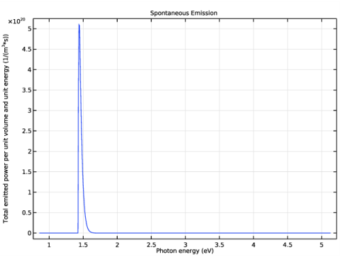
Figure 4 shows the spontaneous emission from the device when the incident wavelength was set to 725 nm. There is no emission with photon energies below the band-gap energy, as expected. At the band-gap energy the emission abruptly begins, peaking with an emitted photon energy of ~1.505 eV which corresponds to a wavelength of 825 nm.
Figure 4: Spontaneous emission from the device when the incident wavelength is set to 725 nm.
Application Library path: Semiconductor_Module/Photonic_Devices_and_Sensors/gaas_pin_photodiode
Modeling Instructions
From the File menu, choose New.
New
In the New window, click  Model Wizard.
Model Wizard
1
In the Model Wizard window, click  2D.
2
In the Select Physics tree, select Semiconductor>Semiconductor Optoelectronics, Frequency Domain.
3
Click Add.
4
Click  Study.
5
In the Select Study tree, select Preset Studies for Selected Multiphysics>Frequency-Stationary.
6
Global Definitions
Parameters 1
Input model parameters. Note in particular the parameters involving the out-of-plane thicknesses since this is a 2D model.
1
In the Model Builder window, under Global Definitions click Parameters 1.
2
In the Settings window for Parameters, locate the Parameters section.
3
Geometry 1
Create the model geometry. The length scale of um is appropriate and the geometry consists of a single rectangle. The physics of this model is 1D in nature with no variation in the horizontal direction. The reason why we use a 2D model is that there is no 1D wave optics interface.
1
In the Model Builder window, under Component 1 (comp1) click Geometry 1.
2
In the Settings window for Geometry, locate the Units section.
3
From the Length unit list, choose µm.
Rectangle 1 (r1)
In the Geometry toolbar, click  Rectangle.
Set the out-of-plane thickness for the semiconductor physics interface to d0 = 1 um (the one for wave optics is hard-coded at 1 m). Switch to Fermi-Dirac carrier statistics, which is appropriate for the high doping concentrations used in this device.
Semiconductor (semi)
1
In the Model Builder window, under Component 1 (comp1) click Semiconductor (semi).
2
In the Settings window for Semiconductor, locate the Thickness section.
3
In the d text field, type d0.
4
Locate the Model Properties section. From the Carrier statistics list, choose Fermi-Dirac.
Geometry 1
Rectangle 1 (r1)
1
In the Model Builder window, under Component 1 (comp1)>Geometry 1 click Rectangle 1 (r1).
2
In the Settings window for Rectangle, locate the Size and Shape section.
3
In the Width text field, type w_dom.
4
In the Height text field, type h_dom.
5
Click  Build All Objects.
Set up the doping, this is achieved with five doping features. Analytic Doping Model features are used to define the background doping and the main p and n sections of the device. Geometric Doping Models are used to create highly doped layers are the top and bottom of the device to increase the efficiency of the metal contacts.
Semiconductor (semi)
Constant p doping
1
In the Physics toolbar, click  Domains and choose Analytic Doping Model.
2
In the Settings window for Analytic Doping Model, type Constant p doping in the Label text field.
3
4
Locate the Impurity section. In the NA0 text field, type 1e14[1/cm^3].
p Doping
1
In the Physics toolbar, click  Domains and choose Analytic Doping Model.
2
In the Settings window for Analytic Doping Model, type p Doping in the Label text field.
3
4
Locate the Distribution section. From the list, choose Box.
5
Locate the Impurity section. In the NA0 text field, type 1e18[1/cm^3].
6
Locate the Uniform Region section. Specify the r0 vector as
7
In the W text field, type w_dom.
8
In the D text field, type 0.1*h_dom.
9
Locate the Profile section. In the dj text field, type 0.15*h_dom.
10
From the Nb list, choose Acceptor concentration (semi/adm1).
p+ Doping
1
In the Physics toolbar, click  Domains and choose Geometric Doping Model.
2
In the Settings window for Geometric Doping Model, type p+ Doping in the Label text field.
3
4
Locate the Impurity section. In the NA0 text field, type 1e20[1/cm^3].
5
Locate the Profile section. In the dj text field, type 0.1*h_dom.
6
From the Nb list, choose Acceptor concentration (semi/adm1).
Boundary Selection for Doping Profile 1
1
In the Model Builder window, expand the p+ Doping node, then click Boundary Selection for Doping Profile 1.
2
n Doping
1
In the Physics toolbar, click  Domains and choose Analytic Doping Model.
2
In the Settings window for Analytic Doping Model, type n Doping in the Label text field.
3
4
Locate the Distribution section. From the list, choose Box.
5
Locate the Impurity section. From the Impurity type list, choose Donor doping (n-type).
6
In the ND0 text field, type 1e18[1/cm^3].
7
Locate the Uniform Region section. In the W text field, type w_dom.
8
In the D text field, type 0.1*h_dom.
9
Locate the Profile section. In the dj text field, type 0.15*h_dom.
10
From the Nb list, choose Acceptor concentration (semi/adm1).
n+ Doping
1
In the Physics toolbar, click  Domains and choose Geometric Doping Model.
2
In the Settings window for Geometric Doping Model, type n+ Doping in the Label text field.
3
4
Locate the Impurity section. From the Impurity type list, choose Donor doping (n-type).
5
In the ND0 text field, type 1e20[1/cm^3].
6
Locate the Profile section. In the dj text field, type 0.1*h_dom.
7
From the Nb list, choose Acceptor concentration (semi/adm1).
Boundary Selection for Doping Profile 1
1
In the Model Builder window, expand the n+ Doping node, then click Boundary Selection for Doping Profile 1.
2
Apply metal contact boundary conditions to the top and bottom surfaces to form the p and n contacts.
p-Contact
1
In the Physics toolbar, click  Boundaries and choose Metal Contact.
2
In the Settings window for Metal Contact, type p-Contact in the Label text field.
3
4
Locate the Terminal section. In the V0 text field, type V_p.
n-Contact
1
In the Physics toolbar, click  Boundaries and choose Metal Contact.
2
In the Settings window for Metal Contact, type n-Contact in the Label text field.
3
4
Locate the Terminal section. In the V0 text field, type V_n.
Add GaAs material from the Semiconductor Material Library and specify the real component of the refractive index.
Add Material
1
In the Home toolbar, click  Add Material to open the Add Material window.
2
Go to the Add Material window.
3
In the tree, select Semiconductors>GaAs - Gallium Arsenide.
4
Click Add to Component in the window toolbar.
5
In the Home toolbar, click  Add Material to close the Add Material window.
Materials
GaAs - Gallium Arsenide (mat1)
1
In the Settings window for Material, locate the Material Contents section.
2
3
Right-click the Refractive index, real part row and choose Edit.
4
In the Refractive index, real part dialog box, type n0 in the text field.
5
6
In the Settings window for Material, locate the Material Contents section.
7
8
Right-click the Refractive index, imaginary part row and choose Edit.
9
In the Refractive index, imaginary part dialog box, type 0 in the text field.
10
With the doping and electrical contacts defined, the next step is to configure the Optical Transitions feature. The default settings are appropriate for this model, all that is required is to set the spontaneous lifetime.
Semiconductor (semi)
Optical Transitions 1
1
In the Model Builder window, under Component 1 (comp1)>Semiconductor (semi) click Optical Transitions 1.
2
In the Settings window for Optical Transitions, locate the Transition Matrix Element section.
3
In the τspon text field, type tau.
Next configure the Electromagnetic Waves, Frequency Domain interface. Two Ports are required, one to excite the top surface of the device with incident radiation and one on the bottom surface to absorb the radiation. This is equivalent to having the electromagnetic wave pass through the device without any reflection from the exit surface. For the first port, the input power parameter Pin assumes the out-of-plane thickness of d0 = 1 um. Scale it up to the out-of-plane thickness of 1[m] as hard-coded by the wave optics interface.
Electromagnetic Waves, Frequency Domain (ewfd)
In the Model Builder window, under Component 1 (comp1) click Electromagnetic Waves, Frequency Domain (ewfd).
Port 1
1
In the Physics toolbar, click  Boundaries and choose Port.
2
3
In the Settings window for Port, locate the Port Properties section.
4
In the Pin text field, type Pin*1[m]/d0.
5
Locate the Port Mode Settings section. Specify the E0 vector as
6
In the β text field, type ewfd.k.
Port 2
1
In the Physics toolbar, click  Boundaries and choose Port.
2
3
In the Settings window for Port, locate the Port Mode Settings section.
4
Specify the E0 vector as
5
In the β text field, type ewfd.k.
Periodic Condition 1
1
In the Physics toolbar, click  Boundaries and choose Periodic Condition.
Add the Periodic Condition feature to the sides of the device. This is equivalent to modeling a section of larger device which has greater lateral extent.
2
Set a nonzero initial value for the electric field.
Initial Values 1
1
In the Model Builder window, click Initial Values 1.
2
In the Settings window for Initial Values, locate the Initial Values section.
3
Specify the E vector as
Configure the mesh, a mapped mesh with only one element in the horizontal direction is used for this effectively 1D model.
Mesh 1
Mapped 1
In the Mesh toolbar, click  Mapped.
Distribution 1
1
Right-click Mapped 1 and choose Distribution.
2
3
In the Settings window for Distribution, locate the Distribution section.
4
In the Number of elements text field, type 1.
Distribution 2
1
In the Model Builder window, right-click Mapped 1 and choose Distribution.
2
3
In the Settings window for Distribution, locate the Distribution section.
4
In the Number of elements text field, type 500.
5
Click  Build All.
Create a nonlocal integration coupling to aid in evaluating the results.
Definitions (comp1)
Integration 1 (intop1)
1
In the Definitions toolbar, click  Nonlocal Couplings and choose Integration.
2
In the Settings window for Integration, locate the Source Selection section.
3
From the Selection list, choose All domains.
4
Locate the Advanced section. In the Integration order text field, type 1.
Configure the study to sweep the wavelength and then compute.
Study 1: Wavelength sweep
1
In the Model Builder window, click Study 1.
2
In the Settings window for Study, type Study 1: Wavelength sweep in the Label text field.
3
Locate the Study Settings section. Clear the Generate default plots check box.
Step 1: Frequency-Stationary
1
In the Model Builder window, under Study 1: Wavelength sweep click Step 1: Frequency-Stationary.
2
In the Settings window for Frequency-Stationary, locate the Study Settings section.
3
In the Frequency text field, type f0.
4
Click to expand the Study Extensions section. Select the Auxiliary sweep check box.
5
6
7
In the Home toolbar, click  Compute.
Plot doping profile of the device and the energy level diagram.
Results
Doping profile
1
In the Home toolbar, click  Add Plot Group and choose 1D Plot Group.
2
In the Settings window for 1D Plot Group, type Doping profile in the Label text field.
3
Locate the Data section. From the Parameter selection (lda0) list, choose First.
Line Graph 1
1
Right-click Doping profile and choose Line Graph.
2
3
In the Settings window for Line Graph, locate the y-Axis Data section.
4
In the Expression text field, type semi.Nd-semi.Na.
5
In the Unit field, type 1/cm^3.
6
Locate the x-Axis Data section. From the Parameter list, choose Reversed arc length.
Doping profile
1
In the Model Builder window, click Doping profile.
2
In the Settings window for 1D Plot Group, locate the Plot Settings section.
3
Select the x-axis label check box.
4
5
In the Doping profile toolbar, click  Plot.
6
Click the  Zoom Extents button in the Graphics toolbar.
Energy level diagram
1
In the Home toolbar, click  Add Plot Group and choose 1D Plot Group.
2
In the Settings window for 1D Plot Group, type Energy level diagram in the Label text field.
3
Locate the Data section. From the Parameter selection (lda0) list, choose Last.
Conduction band
1
Right-click Energy level diagram and choose Line Graph.
2
3
In the Settings window for Line Graph, locate the y-Axis Data section.
4
In the Expression text field, type semi.Ec_e.
5
From the Unit list, choose eV.
6
Locate the x-Axis Data section. From the Parameter list, choose Reversed arc length.
7
Click to expand the Legends section. From the Legends list, choose Manual.
8
9
Select the Show legends check box.
10
In the Label text field, type Conduction band.
Electron Quasi-Fermi energy
1
Right-click Conduction band and choose Duplicate.
2
In the Settings window for Line Graph, type Electron Quasi-Fermi energy in the Label text field.
3
Locate the y-Axis Data section. In the Expression text field, type semi.Efn_e.
4
Locate the Legends section. In the table, enter the following settings:
5
Click to expand the Coloring and Style section. Find the Line style subsection. From the Line list, choose Dashed.
6
From the Color list, choose Blue.
Valence band
1
In the Model Builder window, right-click Conduction band and choose Duplicate.
2
In the Settings window for Line Graph, type Valence band in the Label text field.
3
Locate the y-Axis Data section. In the Expression text field, type semi.Ev_e.
4
Locate the Coloring and Style section. From the Color list, choose Black.
5
Locate the Legends section. In the table, enter the following settings:
Electron Quasi-Fermi energy 1
1
In the Model Builder window, right-click Electron Quasi-Fermi energy and choose Duplicate.
2
In the Settings window for Line Graph, locate the y-Axis Data section.
3
In the Expression text field, type semi.Efp_e.
4
Locate the Coloring and Style section. From the Color list, choose Black.
5
Locate the Legends section. In the table, enter the following settings:
Energy level diagram
1
In the Model Builder window, click Energy level diagram.
2
In the Settings window for 1D Plot Group, locate the Plot Settings section.
3
Select the x-axis label check box.
4
5
Select the y-axis label check box.
6
7
Click to expand the Title section. From the Title type list, choose Manual.
8
In the Title text area, type Energy level diagram.
9
In the Energy level diagram toolbar, click  Plot.
10
Click the  Zoom Extents button in the Graphics toolbar.
Plot the current per input optical power as a function of the wavelength.
Current as a function of wavelength
1
In the Home toolbar, click  Add Plot Group and choose 1D Plot Group.
2
In the Settings window for 1D Plot Group, type Current as a function of wavelength in the Label text field.
Global 1
1
Right-click Current as a function of wavelength and choose Global.
2
In the Settings window for Global, locate the y-Axis Data section.
3
4
Locate the x-Axis Data section. From the Unit list, choose nm.
5
In the Current as a function of wavelength toolbar, click  Plot.
6
Click the  Zoom Extents button in the Graphics toolbar.
Plot the electric field for a wavelength of 725 nm. This wavelength corresponds with the peak in the current.
Electric field
1
In the Home toolbar, click  Add Plot Group and choose 1D Plot Group.
2
In the Settings window for 1D Plot Group, type Electric field in the Label text field.
3
Locate the Data section. From the Parameter selection (lda0) list, choose From list.
4
In the Parameter values (lda0 (m)) list, select 7.25E-7.
Line Graph 1
1
Right-click Electric field and choose Line Graph.
2
3
In the Settings window for Line Graph, locate the x-Axis Data section.
4
From the Parameter list, choose Reversed arc length.
Electric field
1
In the Model Builder window, click Electric field.
2
In the Settings window for 1D Plot Group, locate the Plot Settings section.
3
Select the x-axis label check box.
4
5
Select the y-axis label check box.
6
In the associated text field, type Electric field magnitude (V/m).
7
In the Electric field toolbar, click  Plot.
8
Click the  Zoom Extents button in the Graphics toolbar.
For those who are interested in the conservation of number of particles, we can evaluate the rate of absorption of photons and compare with the rate of charged particles reaching the metal contact terminals. The rate of absorption can be computed in two different ways - either using the S-parameters of the wave optical ports or using the optical transition rates from the semiconductor model. All three rates evaluated below agree reasonably well.
Evaluation Group 1 - check particle conservation
1
In the Results toolbar, click  Evaluation Group.
2
In the Settings window for Evaluation Group, type Evaluation Group 1 - check particle conservation in the Label text field.
3
Locate the Data section. From the Parameter selection (lda0) list, choose From list.
4
In the Parameter values (lda0 (m)) list, select 7.25E-7.
Global Evaluation 1
1
Right-click Evaluation Group 1 - check particle conservation and choose Global Evaluation.
2
In the Settings window for Global Evaluation, locate the Expressions section.
3
4
In the Evaluation Group 1 - check particle conservation toolbar, click  Evaluate.
Plot the spontaneous emission, which in this device is due to unwanted recombination of carriers before they can be swept to the contacts. Although emission is not a design feature of photodiodes, it is useful to plot as an example of how to access quantities from the extra dimension which is used to represent the frequency domain. In order to access this data a new solution is required to hold the data from the extra dimension.
Study 1: Extra dimension
1
In the Results toolbar, click  More Datasets and choose Solution.
2
In the Settings window for Solution, type Study 1: Extra dimension in the Label text field.
3
Locate the Solution section. From the Component list, choose Extra Dimension from Optical Transitions 1 (semi_ot1_xdim).
Spontaneous emission
1
In the Results toolbar, click  1D Plot Group.
2
In the Settings window for 1D Plot Group, type Spontaneous emission in the Label text field.
3
Locate the Data section. From the Dataset list, choose Study 1: Extra dimension (sol1).
4
From the Parameter selection (lda0) list, choose From list.
5
In the Parameter values (lda0 (m)) list, select 7.25E-7.
Line Graph 1
1
Right-click Spontaneous emission and choose Line Graph.
The spontaneous emission data is held in a variable semi.ot1.dP_dE which exists in the extra dimension. This data is plotted using the expression comp1.atxd2(0,0.5e-6,semi.ot1.dP_dE), where the command comp1.atxd#([coord],var) retrieves the data from variable var as a function of the extra dimension from coordinate coord of the model geometry. In this example, the power emitted per unit volume and energy (semi.ot1.dP_dE) is obtained as a function of frequency (the extra dimension) from coordinate (0,0.5 um), which corresponds with the vertical center of the device. The numerical value # is required to let COMSOL know the dimension of the geometry to which the extra dimension is attached, in this case the model geometry is 2D so the value 2 is used. In addition, the tag comp1... tells COMSOL to look at component 1, in models with multiple components this allows for them to be individually addressed.
2
In the Settings window for Line Graph, locate the Selection section.
3
From the Selection list, choose All domains.
4
Locate the y-Axis Data section. In the Expression text field, type comp1.atxd2(0,0.5e-6,semi.ot1.dP_dE).
5
Select the Description check box.
6
In the associated text field, type Total emitted power per unit volume and unit energy.
7
Locate the x-Axis Data section. From the Parameter list, choose Expression.
8
In the Expression text field, type hbar_const*comp1.atxd2(0,0.5e-6,semi.ot1.omega).
9
From the Unit list, choose eV.
10
Select the Description check box.
11
Spontaneous emission
1
In the Model Builder window, click Spontaneous emission.
2
In the Settings window for 1D Plot Group, locate the Title section.
3
From the Title type list, choose Manual.
4
In the Title text area, type Spontaneous Emission.
5
In the Spontaneous emission toolbar, click  Plot.
6
Click the  Zoom Extents button in the Graphics toolbar.