PDF

Caughey-Thomas Mobility
This model demonstrates how to use the Caughey-Thomas high field saturation model for the electron and hole mobility. Field dependent mobility dramatically increases the nonlinearity of the problem. It is necessary to use the continuation study extension to obtain convergence in the high field limit.
Introduction
With an increase in the parallel component of the applied field, carriers can gain energies above the ambient thermal energy and be able to transfer energy gained by the field to the lattice by optical phonon emission. The latter effect leads to a saturation of the carriers mobility.
The Caughey-Thomas mobility model adds high field velocity scattering to an existing mobility model (or to a constant input mobility). The Caughey-Thomas model is based on equations presented in Ref. 1.
The electron (μn,lo) and hole (μp,lo) mobilities are determined by the following equations:
Here T is the lattice temperature, μin,n and μin,p are the electron and hole input mobilities, and Fn and Fp are the driving forces for electrons and holes (currently Fn = E||,n and Fp = E||,p, where E||,n is the component of the electric field parallel to the electron current and E||,p is the component of the electric field parallel to the hole current). All other parameters in the model are material properties (note that v0,n and v0,p are the saturation velocities for electrons and holes and have units of m/s). The material properties for Silicon are also obtained from Ref. 1.
Model Definition
The model represents a simplified 2D MOSFET where the n-doped drain and source are respectively located on the left and right side of the geometry; see Figure 1. The gate is positioned on top of the p-doped silicon section, which is located at the center of the device.
The model consists in sweeping the drain to source voltage form 0 V to 1 V under a gate to source voltage of 0 V. Sweeping the drain voltage creates an important electric field at the left side of the gate at the junction between the n- and p-doped regions. In order to ensure convergence of the nonlinear model, a solver continuation parameter is used to ramp up the electron and hole driving forces (Fn and Fp) as the drain voltage is swept.
Figure 1: Schematic of the modeled device.
Results and Discussion
Figure 2 shows the effect of the Caughey-Thomas mobility model on the solution. The comparison of the constant mobility (the driving forces are multiplied by 1·10-6) and the Caughey-Thomas mobility (Fn and Fp multiplied by 1) models shows a more pronounced saturation effect for the Caughey-Thomas model.
Figure 3 shows that the electron mobility varies substantially along the device. The electron mobility is 3 order of magnitude lower in the vicinity of the drain-gate junction as a consequence of the high electric field generated by the applied potential on the drain contact.
Figure 4 and Figure 5 show the effect of the mobility model on the electron drift velocity. Figure 4 shows the electron drift velocity for the Caughey-Thomas mobility model (Fn and Fp multiplied by 1) and Figure 5 for the constant mobility model (Fn and Fp multiplied by 1·10-6). A comparison of the two figures clearly shows an important reduction of the electron drift velocity when the field effect is taken into account.
Figure 2: Comparison of the terminal current for the constant mobility and Caughey-Thomas mobility. The current is lower and levels off more rapidly due to the fact that the mobility decreases when the electric field is high.
Figure 3: Plot of the electron mobility at a drain-source voltage of 1 V. The mobility varies by 3 orders of magnitude over the modeling domain.
Figure 4: Plot of the electron drift velocity using Caughey-Thomas mobility. The drift velocity can barely exceed 1.15 x 105 m/s.
Figure 5: Plot of the electron drift velocity for the constant mobility case. Since the mobility does not decrease as the electric field increases, the drift velocity becomes very high.
Reference
1. C. Canali, G. Majni, R. Minder, and G. Ottaviani, “Electron and Hole Drift Velocity Measurements in Silicon and Their Empirical Relation to Electric Field and Temperature,” IEEE Transactions on Electron Devices, vol. 22, no. 11, pp. 1045–1047, 1975.
Note: Note the correction in: G. Ottaviani, “Correction to ‘Electron and hole drift velocity measurements in silicon and their empirical relation to electric field and temperatures’,” IEEE Transactions on Electron Devices, vol. 23, no. 9, pp. 1113, 1976.
Application Library path: Semiconductor_Module/Transistors/caughey_thomas_mobility
Modeling Instructions
From the File menu, choose New.
New
In the New window, click  Model Wizard.
Model Wizard
1
In the Model Wizard window, click  2D.
2
In the Select Physics tree, select Semiconductor>Semiconductor (semi).
3
Click Add.
4
Click  Study.
5
In the Select Study tree, select General Studies>Stationary.
6
Global Definitions
Parameters 1
1
In the Model Builder window, under Global Definitions click Parameters 1.
2
In the Settings window for Parameters, locate the Parameters section.
3
Geometry 1
1
In the Model Builder window, under Component 1 (comp1) click Geometry 1.
2
In the Settings window for Geometry, locate the Units section.
3
From the Length unit list, choose nm.
Rectangle 1 (r1)
1
In the Geometry toolbar, click  Rectangle.
2
In the Settings window for Rectangle, locate the Size and Shape section.
3
In the Width text field, type Lg.
4
In the Height text field, type Wfin/2.
Rectangle 2 (r2)
1
In the Geometry toolbar, click  Rectangle.
2
In the Settings window for Rectangle, locate the Size and Shape section.
3
In the Height text field, type Wfin/2.
4
Locate the Position section. In the x text field, type -1.
Rectangle 3 (r3)
1
In the Geometry toolbar, click  Rectangle.
2
In the Settings window for Rectangle, locate the Size and Shape section.
3
In the Height text field, type Wfin/2.
4
Locate the Position section. In the x text field, type Lg.
5
Click  Build All Objects.
Add Material
1
In the Home toolbar, click  Add Material to open the Add Material window.
2
Go to the Add Material window.
3
In the tree, select Semiconductors>Si - Silicon.
4
Click Add to Component in the window toolbar.
5
In the Home toolbar, click  Add Material to close the Add Material window.
Semiconductor (semi)
1
In the Model Builder window, under Component 1 (comp1) click Semiconductor (semi).
2
In the Settings window for Semiconductor, click to expand the Continuation Settings section.
3
In the Cp text field, type ds.
Analytic Doping Model 1
1
In the Physics toolbar, click  Domains and choose Analytic Doping Model.
2
3
In the Settings window for Analytic Doping Model, locate the Impurity section.
4
From the Impurity type list, choose Donor doping (n-type).
5
In the ND0 text field, type 1e19[1/cm^3].
Analytic Doping Model 2
1
In the Physics toolbar, click  Domains and choose Analytic Doping Model.
2
3
In the Settings window for Analytic Doping Model, locate the Impurity section.
4
In the NA0 text field, type 1e15[1/cm^3].
Metal Contact 1
1
In the Physics toolbar, click  Boundaries and choose Metal Contact.
2
3
In the Settings window for Metal Contact, locate the Terminal section.
4
In the V0 text field, type Vds.
Metal Contact 2
1
In the Physics toolbar, click  Boundaries and choose Metal Contact.
2
Thin Insulator Gate 1
1
In the Physics toolbar, click  Boundaries and choose Thin Insulator Gate.
2
3
In the Settings window for Thin Insulator Gate, locate the Terminal section.
4
In the V0 text field, type Vgs.
5
Locate the Gate Contact section. In the εins text field, type 3.9.
6
In the dins text field, type tox.
Semiconductor Material Model 1
In the Model Builder window, click Semiconductor Material Model 1.
Caughey-Thomas Mobility Model (E) 1
1
In the Physics toolbar, click  Attributes and choose Caughey-Thomas Mobility Model (E).
2
In the Settings window for Caughey-Thomas Mobility Model (E), click to expand the Continuation Settings section.
3
From the Continuation type list, choose Use interface continuation parameter.
Semiconductor Material Model 1
1
In the Model Builder window, click Semiconductor Material Model 1.
2
In the Settings window for Semiconductor Material Model, locate the Mobility Model section.
3
From the μn list, choose Electron mobility, Caughey-Thomas (semi/smm1/mmct1).
4
From the μp list, choose Hole mobility, Caughey-Thomas (semi/smm1/mmct1).
5
In the Model Builder window, click Semiconductor (semi).
6
In the Settings window for Semiconductor, click to expand the Discretization section.
7
From the Formulation list, choose Finite element, log formulation (linear shape function).
Set up a user-defined mesh.
Mesh 1
Mapped 1
1
In the Mesh toolbar, click  Mapped.
2
In the Settings window for Mapped, click to expand the Reduce Element Skewness section.
3
Select the Adjust edge mesh check box.
Distribution 1
1
Right-click Mapped 1 and choose Distribution.
2
3
In the Settings window for Distribution, locate the Distribution section.
4
From the Distribution type list, choose Predefined.
5
In the Number of elements text field, type 20.
6
In the Element ratio text field, type 5.
7
From the Growth formula list, choose Geometric sequence.
8
Select the Reverse direction check box.
Distribution 2
1
In the Model Builder window, right-click Mapped 1 and choose Distribution.
2
Distribution 3
1
Right-click Mapped 1 and choose Distribution.
2
3
In the Settings window for Distribution, locate the Distribution section.
4
From the Distribution type list, choose Predefined.
5
In the Number of elements text field, type 50.
6
In the Element ratio text field, type 25.
7
From the Growth formula list, choose Geometric sequence.
8
Select the Symmetric distribution check box.
Study 1
Step 1: Stationary
Set up an auxiliary continuation sweep for the ds parameter.
1
In the Model Builder window, under Study 1 click Step 1: Stationary.
2
In the Settings window for Stationary, click to expand the Study Extensions section.
3
Select the Auxiliary sweep check box.
4
5
6
7
8
From the Sweep type list, choose All combinations.
9
From the Reuse solution from previous step list, choose Auto.
Solution 1 (sol1)
1
In the Study toolbar, click  Show Default Solver.
2
In the Model Builder window, expand the Solution 1 (sol1) node.
3
In the Model Builder window, expand the Study 1>Solver Configurations>Solution 1 (sol1)>Stationary Solver 1 node.
4
Right-click Parametric 1 and choose Previous Solution.
5
In the Settings window for Previous Solution, locate the Previous Solution section.
6
Under Variables, click  Add.
7
In the Add dialog box, in the Variables list, choose Electric field parallel to electron current density (comp1.semi.smm1.mmct1.Epn) and Electric field parallel to hole current density (comp1.semi.smm1.mmct1.Epp).
8
9
In the Study toolbar, click  Compute.
Results
Electron Concentration (semi)
Click the  Zoom Extents button in the Graphics toolbar.
1D Plot Group 4
1
In the Home toolbar, click  Add Plot Group and choose 1D Plot Group.
2
In the Settings window for 1D Plot Group, locate the Data section.
3
From the Parameter selection (ds) list, choose From list.
4
In the Parameter values (ds) list, choose 1E-6 and 1.001.
Global 1
1
Right-click 1D Plot Group 4 and choose Global.
2
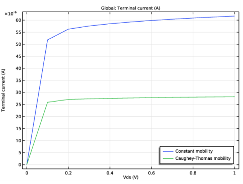
In the Settings window for Global, click Replace Expression in the upper-right corner of the y-Axis Data section. From the menu, choose Component 1 (comp1)>Semiconductor>Terminals>semi.I0_1 - Terminal current - A.
3
Locate the x-Axis Data section. From the Axis source data list, choose Vds.
4
In the 1D Plot Group 4 toolbar, click  Plot.
5
Click to expand the Legends section. From the Legends list, choose Manual.
6
7
In the 1D Plot Group 4 toolbar, click  Plot.
8
Click the  Zoom Extents button in the Graphics toolbar.
1D Plot Group 4
1
In the Model Builder window, click 1D Plot Group 4.
2
In the Settings window for 1D Plot Group, locate the Legend section.
3
From the Position list, choose Lower right.
2D Plot Group 5
In the Home toolbar, click  Add Plot Group and choose 2D Plot Group.
Surface 1
1
Right-click 2D Plot Group 5 and choose Surface.
2
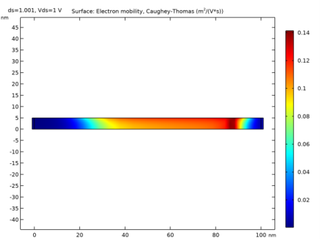
In the Settings window for Surface, click Replace Expression in the upper-right corner of the Expression section. From the menu, choose Component 1 (comp1)>Semiconductor>Mobility>semi.mun_ct - Electron mobility, Caughey-Thomas - m²/(V·s).
3
In the 2D Plot Group 5 toolbar, click  Plot.
4
Click the  Zoom Extents button in the Graphics toolbar.
2D Plot Group 6
In the Model Builder window, under Results right-click 2D Plot Group 5 and choose Duplicate.
Surface 1
1
In the Model Builder window, expand the 2D Plot Group 6 node, then click Surface 1.
2
In the Settings window for Surface, locate the Expression section.
3
In the Expression text field, type semi.mun_ct*semi.EX.
4
Select the Description check box.
5
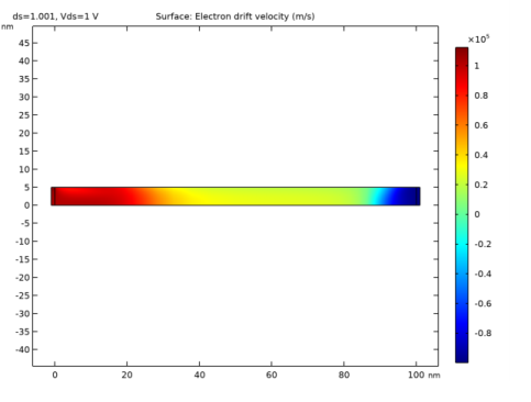
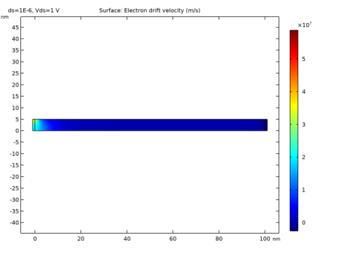
In the associated text field, type Electron drift velocity.
6
In the 2D Plot Group 6 toolbar, click  Plot.
7
Click the  Zoom Extents button in the Graphics toolbar.
2D Plot Group 6
1
In the Model Builder window, click 2D Plot Group 6.
2
In the Settings window for 2D Plot Group, locate the Data section.
3
From the Parameter value (ds) list, choose 1E-6.
4
In the 2D Plot Group 6 toolbar, click  Plot.
5
Click the  Zoom Extents button in the Graphics toolbar.