PDF

Designing a Waveguide Diplexer for the 5G Mobile Network
Introduction
A diplexer is a device that combines or splits signals into two different frequency bands, widely used in mobile communication systems. This example simulates splitting properties using a simplified 2D geometry. The computed S-parameters and electric fields at the lower and upper bands will show the diplexer characteristics in the Ka-band.
Figure 1: 2D layout of the diplexer composed of 3-port waveguide structures.
Model Definition
This example is based on a WR-28 waveguide for Ka-band applications. The width of the 2D waveguide is 0.28 inches, which is the length of the longer side of a WR-28 waveguide aperture. The model considers only the dominant TE1 mode. The cutoff frequency of the dominant mode is 21.08 GHz. There are two cavities working as bandpass structures between the input and each output port that are connected with irises. The waveguides, cavities and irises are modeled as copper with finite conductivity using an Impedance Boundary condition to evaluate loss at a high frequency range and the inside of the waveguide is filled with air. On each end of the waveguide, a port boundary condition is applied with the predefined rectangular TE1 mode. Only one port is excited to observe the S-parameters of the example.
Results and Discussion
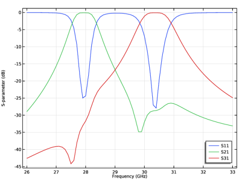
S-parameters are plotted in Figure 2. The lower passband is around 28 GHz and the upper passband is around 30.4 GHz. The insertion loss in each passband is about 0.1 dB, mainly caused by the finite conductivity of the copper walls. In Figure 3 and Figure 4, the E-field norm is visualized for each passband, showing that the input power at each passband is not split into two output ports, but separately distributed without being coupled to the other port.
Figure 2: The S-parameter plot shows the lower and upper passband of the diplexer.
The isolation properties between two output ports are not reviewed in this example but users are encouraged to try by exciting port 2 or 3 only.
Figure 3: The E-field norm plot for a frequency of 28 GHz. The input power flows into port 2 only.
Figure 4: The E-field norm plot for a frequency of 30.4 GHz. The input power flows into port 3 only.
Application Library path: RF_Module/Filters/waveguide_diplexer
Modeling Instructions
From the File menu, choose New.
New
In the New window, click  Model Wizard.
Model Wizard
1
In the Model Wizard window, click  2D.
2
In the Select Physics tree, select Radio Frequency>Electromagnetic Waves, Frequency Domain (emw).
3
Click Add.
4
Click  Study.
5
In the Select Study tree, select General Studies>Frequency Domain.
6
Study 1
Step 1: Frequency Domain
1
In the Model Builder window, under Study 1 click Step 1: Frequency Domain.
2
In the Settings window for Frequency Domain, locate the Study Settings section.
3
In the Frequencies text field, type range(26[GHz],0.1[GHz],33[GHz]).
Geometry 1
1
In the Model Builder window, under Component 1 (comp1) click Geometry 1.
2
In the Settings window for Geometry, locate the Units section.
3
From the Length unit list, choose mm.
Import 1 (imp1)
1
In the Home toolbar, click  Import.
2
In the Settings window for Import, locate the Import section.
3
Click Browse.
4
5
Click Import.
Definitions
Waveguide walls
1
In the Definitions toolbar, click  Explicit.
2
In the Settings window for Explicit, type Waveguide walls in the Label text field.
3
Locate the Input Entities section. From the Geometric entity level list, choose Boundary.
4
Click  Paste Selection.
5
In the Paste Selection dialog box, type 2-54, 57-78 in the Selection text field.
6
Add Material
1
In the Home toolbar, click  Add Material to open the Add Material window.
2
Go to the Add Material window.
3
4
Click Add to Component in the window toolbar.
5
In the tree, select Built-in>Copper.
6
Click Add to Component in the window toolbar.
7
In the Home toolbar, click  Add Material to close the Add Material window.
Materials
Copper (mat2)
1
In the Settings window for Material, locate the Geometric Entity Selection section.
2
From the Geometric entity level list, choose Boundary.
3
From the Selection list, choose Waveguide walls.
Electromagnetic Waves, Frequency Domain (emw)
Port 1
1
In the Model Builder window, under Component 1 (comp1) right-click Electromagnetic Waves, Frequency Domain (emw) and choose Port.
2
3
In the Settings window for Port, locate the Port Properties section.
4
From the Type of port list, choose Rectangular.
For the first port, wave excitation is on by default.
Port 2
1
In the Physics toolbar, click  Boundaries and choose Port.
2
3
In the Settings window for Port, locate the Port Properties section.
4
From the Type of port list, choose Rectangular.
5
Port 3
1
Right-click Port 2 and choose Duplicate.
2
In the Settings window for Port, locate the Boundary Selection section.
3
Click  Clear Selection.
4
With TE waves, only the z-component of the electric field needs to be solved for
5
In the Model Builder window, click Electromagnetic Waves, Frequency Domain (emw).
6
In the Settings window for Electromagnetic Waves, Frequency Domain, locate the Components section.
7
From the Electric field components solved for list, choose Out-of-plane vector.
Impedance Boundary Condition 1
1
In the Physics toolbar, click  Boundaries and choose Impedance Boundary Condition.
2
In the Settings window for Impedance Boundary Condition, locate the Boundary Selection section.
3
From the Selection list, choose Waveguide walls.
Mesh 1
1
In the Model Builder window, under Component 1 (comp1) click Mesh 1.
2
In the Settings window for Mesh, locate the Physics-Controlled Mesh section.
3
From the Element size list, choose Fine.
4
In the Home toolbar, click  Build Mesh.
It is not necessary to review the mesh, but it is a good practice to take a look at it before running the simulation.
Study 1
Step 1: Frequency Domain
Click  Compute.
Results
Contour 1
1
Right-click Electric Field (emw) and choose Contour.
2
In the Settings window for Contour, locate the Coloring and Style section.
3
From the Contour type list, choose Filled.
Height Expression 1
1
Right-click Contour 1 and choose Height Expression.
2
In the Settings window for Height Expression, locate the Axis section.
3
Select the Scale factor check box.
4
5
In the Electric Field (emw) toolbar, click  Plot.
6
Click the  Zoom Extents button in the Graphics toolbar.
The E-field norm is visualized at the last frequency, which is out of the passband. The plot shows that the input wave does not propagate to any of the output ports.
S-parameter (emw)
1
In the Model Builder window, click S-parameter (emw).
2
In the Settings window for 1D Plot Group, locate the Legend section.
3
From the Position list, choose Lower right.
Compare the reproduced plot to Figure 2. The lower and upper passband frequencies are around 28 GHz, and 30.4 GHz, respectively.
Smith Plot (emw)
Electric Field (emw)
1
In the Model Builder window, click Electric Field (emw).
2
In the Settings window for 2D Plot Group, locate the Data section.
3
From the Parameter value (freq (GHz)) list, choose 28.
4
In the Electric Field (emw) toolbar, click  Plot.
The E-field norm plot at the lower passband is shown in Figure 3.
5
From the Parameter value (freq (GHz)) list, choose 30.4.
6
In the Electric Field (emw) toolbar, click  Plot.
Finish the result analysis by reproducing Figure 4, which is the E-field norm plot at the upper passband.