PDF

Step-Index Fiber
Introduction
The transmission speed of optical waveguides is superior to microwave waveguides because optical devices have a much higher operating frequency than microwaves, enabling a far higher bandwidth.
Today the silica glass (SiO2) fiber is forming the backbone of modern communication systems. Before 1970, optical fibers suffered from large transmission losses, making optical communication technology merely an academic issue. In 1970, researchers showed, for the first time, that low-loss optical fibers really could be manufactured. Earlier losses of 2000 dB/km now went down to 20 dB/km. Today’s fibers have losses near the theoretical limit of 0.16 dB/km at 1.55 μm (infrared light).
One of the winning devices has been the single-mode fiber, having a step-index profile with a higher refractive index in the center core and a lower index in the outer cladding. Numerical software plays an important role in the design of single-mode waveguides and fibers. For a fiber cross section, even the simplest shape is difficult and cumbersome to deal with analytically. A circular step-index waveguide is a basic shape where benchmark results are available (see Ref. 1).
This example is a model of a single step-index waveguide made of silica glass. The inner core is made of pure silica glass with refractive index n1 = 1.4457 and the cladding is doped with a refractive index of n2 = 1.4378. These values are valid for free-space wavelengths of 1.55 μm. The radius of the cladding is chosen to be large enough so that the field of confined modes is zero at the exterior boundaries.
For a confined mode there is no energy flow in the radial direction, so the wave must be evanescent in the radial direction in the cladding. This is true only if
On the other hand, the wave cannot be radially evanescent in the core region. Thus
The waves are more confined when neff is close to the upper limit in this interval.
Model Definition
The mode analysis is made on a cross section in the xy-plane of the fiber. The wave propagates in the z direction and has the form
where ω is the angular frequency and β the propagation constant. An eigenvalue equation for the electric field E is derived from Helmholtz equation
which is solved for the eigenvalue λ = jβ.
As boundary condition along the outside of the cladding, the electric field is set to zero. Because the amplitude of the field decays rapidly as a function of the radius of the cladding this is a valid boundary condition.
Results and Discussion
When studying the characteristics of optical waveguides, the effective mode index of a confined mode,
as a function of the frequency is an important characteristic. A common notion is the normalized frequency for a fiber. This is defined as
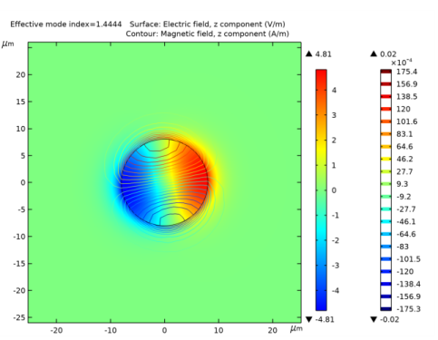
where a is the radius of the core of the fiber. For this simulation, the effective mode index for the fundamental mode, 1.4444 corresponds to a normalized frequency of 4.895. The longitudinal components of the electric and magnetic fields for this mode is shown in Figure 1 below.
Figure 1: The surface plot visualizes the z component of the electric field. This plot is for the effective mode index 1.4444.
Reference
1. A. Yariv, Optical Electronics in Modern Communications, 5th ed., Oxford University Press, 1997.
Application Library path: RF_Module/Tutorials/step_index_fiber
Modeling Instructions
From the File menu, choose New.
New
In the New window, click  Model Wizard.
Model Wizard
1
In the Model Wizard window, click  2D.
2
In the Select Physics tree, select Radio Frequency>Electromagnetic Waves, Frequency Domain (emw).
3
Click Add.
4
Click  Study.
5
In the Select Study tree, select Preset Studies for Selected Physics Interfaces>Mode Analysis.
6
Geometry 1
1
In the Model Builder window, under Component 1 (comp1) click Geometry 1.
2
In the Settings window for Geometry, locate the Units section.
3
From the Length unit list, choose µm.
Circle 1 (c1)
1
In the Geometry toolbar, click  Circle.
2
In the Settings window for Circle, locate the Size and Shape section.
3
In the Radius text field, type 40.
4
Click  Build Selected.
Circle 2 (c2)
1
In the Geometry toolbar, click  Circle.
2
In the Settings window for Circle, locate the Size and Shape section.
3
In the Radius text field, type 8.
4
Click  Build Selected.
Materials
Doped Silica Glass
1
In the Model Builder window, under Component 1 (comp1) right-click Materials and choose Blank Material.
2
In the Settings window for Material, type Doped Silica Glass in the Label text field.
3
4
Click to expand the Material Properties section. In the Material properties tree, select Electromagnetic Models>Refractive index>Refractive index, real part (n).
5
Click  Add to Material.
6
Locate the Material Contents section. In the table, enter the following settings:
Silica Glass
1
Right-click Materials and choose Blank Material.
2
In the Settings window for Material, type Silica Glass in the Label text field.
3
4
Click to expand the Material Properties section. In the Material properties tree, select Electromagnetic Models>Refractive index>Refractive index, real part (n).
5
Click  Add to Material.
6
Locate the Material Contents section. In the table, enter the following settings:
Electromagnetic Waves, Frequency Domain (emw)
Keep the default physics settings, which include perfect electric conductor conditions for the outer boundaries.
Wave Equation, Electric 1
1
In the Model Builder window, under Component 1 (comp1)>Electromagnetic Waves, Frequency Domain (emw) click Wave Equation, Electric 1.
2
In the Settings window for Wave Equation, Electric, locate the Electric Displacement Field section.
3
From the Electric displacement field model list, choose Refractive index.
Mesh 1
1
In the Model Builder window, under Component 1 (comp1) click Mesh 1.
2
In the Settings window for Mesh, locate the Physics-Controlled Mesh section.
3
In the table, clear the Use check box for Electromagnetic Waves, Frequency Domain (emw).
4
From the Element size list, choose Finer.
5
Click  Build All.
Study 1
Step 1: Mode Analysis
1
In the Model Builder window, under Study 1 click Step 1: Mode Analysis.
2
In the Settings window for Mode Analysis, locate the Study Settings section.
3
Select the Search for modes around check box.
4
The modes of interest have an effective mode index somewhere between the refractive indices of the two materials. The fundamental mode has the highest index. Therefore, setting the mode index to search around to something just above the core index guarantees that the solver will find the fundamental mode.
5
In the Mode analysis frequency text field, type c_const/1.55[um]. This frequency corresponds to a free space wavelength of 1.55 μm.
6
In the Home toolbar, click  Compute.
Results
Electric Field (emw)
1
Click the  Zoom Extents button in the Graphics toolbar.
2
Click the  Zoom In button in the Graphics toolbar.
The default plot shows the distribution of the norm of the electric field for the highest of the 6 computed modes (the one with the lowest effective mode index).
To study the fundamental mode, choose the highest mode index. Because the magnetic field is exactly 90 degrees out of phase with the electric field you can see both the magnetic and the electric field distributions by plotting the solution at a phase angle of 45 degrees.
Study 1/Solution 1 (sol1)
1
In the Model Builder window, expand the Results>Datasets node, then click Study 1/Solution 1 (sol1).
2
In the Settings window for Solution, locate the Solution section.
3
In the Solution at angle (phase) text field, type 45.
Electric Field (emw)
1
In the Model Builder window, click Electric Field (emw).
2
In the Settings window for 2D Plot Group, locate the Data section.
3
From the Effective mode index list, choose 1.4444.
Surface
1
In the Model Builder window, expand the Electric Field (emw) node, then click Surface.
2
In the Settings window for Surface, click Replace Expression in the upper-right corner of the Expression section. From the menu, choose Component 1 (comp1)>Electromagnetic Waves, Frequency Domain>Electric>Electric field - V/m>emw.Ez - Electric field, z component.
3
In the Electric Field (emw) toolbar, click  Plot.
Add a contour plot of the H-field.
Contour 1
1
In the Model Builder window, right-click Electric Field (emw) and choose Contour.
2
In the Settings window for Contour, click Replace Expression in the upper-right corner of the Expression section. From the menu, choose Component 1 (comp1)>Electromagnetic Waves, Frequency Domain>Magnetic>Magnetic field - A/m>emw.Hz - Magnetic field, z component.
3
In the Electric Field (emw) toolbar, click  Plot.
The distribution of the transversal E and H field components confirms that this is the HE11 mode. Compare the resulting plot with that in Figure 1.