PDF

Modeling of a Phased Array Antenna
Introduction
The demand for phased array antennas increases not only for the traditional military industry but also in commercial areas such 5G mobile network platforms, Internet of Things (IoT), and satellite communication applications. This example shows how to design a phased array with a beam scanning functionality based on the arithmetic phase difference between the array elements. The initial complicated model can be reduced to a simple single unit cell model with periodic conditions to make the analysis faster and more efficient. Two phased array designs built with microstrip patch antennas are studied and they are in good agreement of the antenna gain.
Figure 1: 8-by-4 antenna array with the far-field radiation pattern in dB scale. The main beam is 30 degrees tilted from the normal z-axis. The electric field norm on the antenna substrate is also visualized.
Model Definition
This example consists of three parts:
Antenna Geometry Part
When a simulation model has repeated geometry designs, it would be cumbersome to draw that geometry over and over again. If there is a predefined geometry frequently used, the modeling process can be more efficient. The RF Module includes the part library consisting of many standard parts and geometries. They are various types of connectors, surface mount device footprints, and rectangular waveguides. You can also create your own customized parts, and use them multiple times in the same or different models.
The part in this model describes a parametrized microstrip patch antenna geometry. Thereby you can easily change the geometry. The design parameters define the size of the substrate, patch radiator, feed line, and impedance matching geometry.
8-by-4 Full Antenna Array
The full antenna array geometry is built with the customized part and array operation. The array substrate is enclosed by a surrounding air domain. All antenna elements are excited by lumped ports with the same default voltage and 50 Ω reference impedance. The arithmetic phase values are used to steer the direction of the main radiation.
By running a parametric sweep of phi shown in Table 1, the beam scanning capability of the phased array antenna can be evaluated.
Figure 2: Lumped port phase configuration on the top view of the antenna array geometry.
For far-field analyses such as radiation pattern, gain, directivity, and effective isotropically radiated power (EIRP), a far-field domain and calculation features are required. It is important to apply the domain feature to the surrounding air domain or connected domains characterized by homogeneous material properties. The far-field calculation boundaries are the exterior boundaries of the far-field domain feature by default.
A perfect electric conductor (PEC) boundary condition is by default applied to the exterior boundaries of the simulation domain. In this model, that boundary condition is overridden by a first-order scattering boundary condition. The scattering boundary condition absorbs all outgoing radiation from the antenna.
The simulation frequency is not high enough to consider the loss coming from the finite conductivity of the copper layers. All metal boundaries are defined using the perfect electric conductor (PEC). The 60 mil dielectric substrate is assumed to be lossless and the relative permittivity, dielectric constant of the material is 3.38 in this model.
Simplified Model Using Periodic Conditions
The complexity of the full antenna array model can be reduced using periodic conditions and it is possible to estimate the far-field radiation pattern of the full antenna array efficiently by utilizing the built-in array factor function.
The periodic conditions are the core features virtually making the unit cell as an infinite array and simplify the original model for the faster analysis. Each periodic condition has a pair of boundary selections facing each other that can be identified as the source and destination boundaries, respectively. Four side boundaries are configured in two periodic conditions. The Floquet periodicity correlates the source and destination boundaries with a user-specified phase in terms of k-vector. The k-vector for Floquet periodicity is extracted using the direction of the main beam steered by the arithmetic phase progression. The beam is steered only around the y-axis. So the Floquet periodicity type is used for the periodic condition in which the selections are normal to the x-axis. In the other periodic condition where the boundaries are normal to the y-axis, the Continuity type is appropriate because no phase variation is expected between the source and the destination boundaries.
The top of the simulation domain is covered by a scattering boundary condition to model the surface as open space. The far-field domain feature is used only in the top air domain. This is a very special case not following the rule of thumb regarding the proper usage of the far-field feature. The basic assumptions here are that
Even if these conditions are fulfilled, this approach has to be carefully applied. In this example, the computed results are compared to those of the full array model and accepted as an alternative method for evaluating the performance of the antenna array for the given design.
Though the unit cell simulation includes the coupling by the adjacent surrounding array elements through the periodic conditions, the far-field transformation is performed only with the unit cell. The computed far-field radiation pattern does not describe that of the complete array. The desired radiation pattern of the array can be approximated by multiplying an array factor to the far field of the single antenna.
The 3D full-wave simulation for an antenna array is memory intensive. By using an asymptotic approach, such as multiplying the far-field of a single antenna with a uniform array factor, the radiation pattern of an antenna array can be evaluated quickly.
The 3D uniform array factor function is available under Definitions>Functions from the postprocessing context menu when a Far-Field Calculation feature is defined in the physics interface. The function call signature is
af3(nx, ny, nz, dx, dy, dz, alphax, alphay, alphaz),
where nx, ny, and nz are the number of elements along the x-, y-, and z-axis, respectively. The arguments dx, dy, and dz are the distances between array elements in terms of wavelength. alphax, alphay, and alphaz are the phase progression in radians.
To evaluate the realized gain of a virtual 8-by-4 antenna array from the realized gain of a single antenna, the following expression is used:
emw2.rGaindBEfar+20*log10(emw2.af3(8,4,1,0.48,0.48,0,-2*pi*0.48*cos(phi),0,0))+10*log10(1/32)
Since it is the dB scale, the multiplication of the array factor represents a summation in the expression.
It assumes that the array is excited by a single input uniform distribution network, so the input power needs to be scaled by a factor 10*log10(1/total number of elements). The direction of the main beam can be steered by defining nonzero phase progression in the uniform array factor. The maximum radiation direction of the array factor along the x-axis is defined by the angle from the x-axis in the phase progression using
The antenna is excited by a uniform lumped port. The lumped port is proper to use on a small boundary where a constant phase is expected over the port boundary.
Results and Discussion
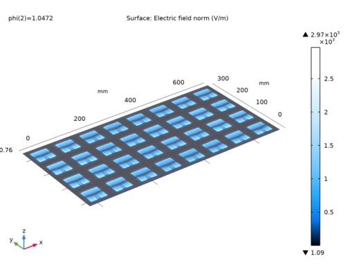
Figure 3 visualizes the electric field norm when all antenna elements are excited with the same voltage, but the arithmetic phase progression is set to have the maximum radiation direction tilted from the z-axis. Strong field intensity is observed around the radiating edges of the patch antennas. Since the norm is plotted, the phase variation is not shown. To see the field variation at each column of the array, a complex-valued field component, Ez, is used in Figure 4. Only the real part of complex values is plotted.
Figure 3: Electric field norm is plotted on the top surface on the antenna array board using a selection subfeature.
Figure 4: Ez plot showing the color variation at each array column.
 
Figure 5 visualizes the far-field radiation pattern in a polar plot. The polar plot format is convenient for checking intuitively the directional properties of an antenna. When there is no phase difference among the excitation ports and all antenna elements are uniformly fed, the generated radiation pattern is normal to the array plane (blue in Figure 5). Though the phase at each port is defined as -2*pi*0.48*cos(phi), the input argument is effectively zero with a parameter phi value of π/2. When phi is π/3, the arithmetic phase applied to each array column group is listed in Table 3.
Figure 5: Far-field polar plot in dB scale for two cases: the beam steering angle at  π/2 and π/3, respectively. When all antenna elements are excited by lumped ports with equal magnitude and zero phases, the main radiation is toward the antenna boresight (blue). When the arithmetic phase progression is applied, the beam can be steered (green).
A reasonably well-designed antenna array may have sidelobe levels below 10 dB which is not conspicuous when they are plotted in linear scale. The dB scale used in the polar plot and 3D far-field radiation pattern (Figure 6) makes the sidelobes more visible. For high-gain antennas, it is recommended to use a finer resolution for the radiation pattern visualization to characterize nulls and sidelobes without missing them. The number of angles in the settings window controls the resolution.
Figure 6: 3D far-field radiation pattern. The main beam direction is tilted from π/3 from the array plane.
The antenna performance for the simplified model is compared to that of the 8-by-4 full array model in Figure 7. The main beam and several sidelobes for both straight and tilted beam cases of the simplified model coincide in angle and level with the results of the full array model. However, there is a noticeable discrepancy in the backward radiationthose below the ground plane. So, this reduced model using the periodic conditions is valid only when approximating the antenna boresight radiation.
Figure 8 shows a similar type of comparison but using the realized gain in the 1D plot. As stated above, a good agreement is observed between two modeling approaches regardless of the beam scanning angle if only the main beam and major sidelobes are of interest for the antenna analysis.
Figure 7: Gain comparison in a polar plot between two modeling methods. The main beam and sidelobe levels are agreed well.
Figure 8: Gain comparison in a 1D plot. 1D plot perspective, different from the polar plot, provides a better view while observing nulls and backlobes.
Notes About the COMSOL Implementation
The first full model may require more than 25GB memory. It is advised to skip the computation and try from the second reduced model if the memory resource is not sufficient.
References
1. https://www.comsol.com/blogs/using-perfectly-matched-layers-and-scattering-boundary-conditions-for-wave-electromagnetics-problems
2. https://www.comsol.com/blogs/how-to-synthesize-the-radiation-pattern-of-an-antenna-array
Application Library path: RF_Module/Antenna_Arrays/microstrip_patch_antenna_periodic
Modeling Instructions
This example consists of two simulations. One is a full 8-by-4 array model, and the other is simplified using periodic conditions. In these two cases, the patch antenna geometry is repeatedly used. So, it would be convenient to build a part that we can add on geometry at any time we need.
From the File menu, choose New.
New
In the New window, click  Model Wizard.
Model Wizard
1
In the Model Wizard window, click  3D.
2
In the Select Physics tree, select Radio Frequency>Electromagnetic Waves, Frequency Domain (emw).
3
Click Add.
4
Click  Study.
5
In the Select Study tree, select General Studies>Frequency Domain.
6
Global Definitions
Parameters 1
1
In the Model Builder window, under Global Definitions click Parameters 1.
2
In the Settings window for Parameters, locate the Parameters section.
3
The unit mil, used for substrate thickness, refers to milliinch. c_const is a predefined COMSOL constant for the speed of light in vacuum.
Antenna Geometry Part
Patch Antenna
1
In the Model Builder window, right-click Global Definitions and choose Geometry Parts>3D Part.
2
In the Settings window for Part, type Patch Antenna in the Label text field.
3
Locate the Units section. From the Length unit list, choose mm.
4
In the Model Builder window, click Patch Antenna.
5
Locate the Input Parameters section. In the table, enter the following settings:
The 50-ohm microstrip line width is set by the thickness and dielectric constant of the substrate. This has to be properly adjusted when using a different substrate for the antenna design. The size of a single antenna unit is based on the array periodicity. We use 0.48 wavelengths in free space to have a relatively high gain and low sidelobes.
Substrate
1
In the Geometry toolbar, click  Block.
2
In the Settings window for Block, type Substrate in the Label text field.
3
Locate the Size and Shape section. In the Width text field, type w_sub.
4
In the Depth text field, type l_sub.
5
In the Height text field, type d.
6
Locate the Position section. From the Base list, choose Center.
Patch
1
In the Geometry toolbar, click  Block.
2
In the Settings window for Block, locate the Size and Shape section.
3
In the Width text field, type w_patch.
4
In the Depth text field, type l_patch.
5
In the Height text field, type d.
6
Locate the Position section. From the Base list, choose Center.
7
In the Label text field, type Patch.
Stub
1
In the Geometry toolbar, click  Block.
2
In the Settings window for Block, type Stub in the Label text field.
3
Locate the Size and Shape section. In the Width text field, type w_stub.
4
In the Depth text field, type l_stub.
5
In the Height text field, type d.
6
Locate the Position section. From the Base list, choose Center.
7
In the x text field, type w_stub/2+w_line/2.
8
In the y text field, type l_stub/2-l_patch/2.
Copy 1 (copy1)
1
In the Geometry toolbar, click  Transforms and choose Copy.
2
3
In the Settings window for Copy, locate the Displacement section.
4
In the x text field, type -w_stub-w_line.
5
Click  Build Selected.
Difference 1 (dif1)
1
In the Geometry toolbar, click  Booleans and Partitions and choose Difference.
2
3
In the Settings window for Difference, locate the Difference section.
4
Find the Objects to subtract subsection. Select the  Activate Selection toggle button.
5
Select the objects blk3 and copy1 only.
By truncating the rectangular patch with two small pieces of rectangular blocks, it creates an antenna feed line and an appropriate feeding point inside the patch without adding an impedance matching network. The characteristic impedance of this microstrip line is about 50 ohm.
Union 1 (uni1)
1
In the Geometry toolbar, click  Booleans and Partitions and choose Union.
2
Click in the Graphics window and then press Ctrl+A to select both objects.
3
In the Geometry toolbar, click  Build All.
8-by-4 Full Antenna Array
Geometry 1
1
In the Model Builder window, under Component 1 (comp1) click Geometry 1.
2
In the Settings window for Geometry, locate the Units section.
3
From the Length unit list, choose mm.
The first full array model may require more than 25GB memory. If the computational resource is not big enough, skip the first full array model and start from the second simplified model. The solved model is available from the menu item File > Application Libraries > Update COMSOL Application Libraries on the menu.
Add the antenna geometry from the part.
Patch Antenna 1 (pi1)
1
In the Geometry toolbar, click  Parts and choose Patch Antenna.
2
In the Settings window for Part Instance, click  Build Selected.
Array 1 (arr1)
1
In the Geometry toolbar, click  Transforms and choose Array.
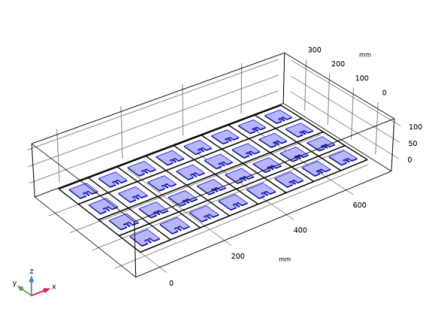
Create an 8-by-4 array using the Array operation from the geometry context menu. The array displacement corresponds to the single antenna size defined in the part.
2
3
In the Settings window for Array, locate the Input section.
4
Find the Input objects subsection. Select the  Activate Selection toggle button.
5
Locate the Size section. In the x size text field, type 8.
6
In the y size text field, type 4.
7
Locate the Displacement section. In the x text field, type lda048.
8
In the y text field, type lda048.
9
Click  Build Selected.
The Wireframe rendering provides the view of interior.
10
Click the  Wireframe Rendering button in the Graphics toolbar.
Add a block for the air domain
Block 1 (blk1)
1
In the Geometry toolbar, click  Block.
2
In the Settings window for Block, locate the Size and Shape section.
3
In the Width text field, type lda048*9.
4
In the Depth text field, type lda048*5.
5
In the Height text field, type 160.
6
Locate the Position section. In the x text field, type -lda048.
7
In the y text field, type -lda048.
8
In the z text field, type -160/2+50.
9
In the Geometry toolbar, click  Build All.
10
Click the  Zoom Extents button in the Graphics toolbar.
Materials
Add a built-in air material for the entire simulation domain.
Add Material
1
In the Home toolbar, click  Add Material to open the Add Material window.
2
Go to the Add Material window.
3
4
Click Add to Component in the window toolbar.
5
In the Home toolbar, click  Add Material to close the Add Material window.
Materials
Override the substrate domain with a dielectric material, where the relative permittivity is set to 3.38.
Substrate
1
In the Model Builder window, under Component 1 (comp1) right-click Materials and choose Blank Material.
2
In the Settings window for Material, type Substrate in the Label text field.
3
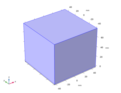
Select Domains 2–65 only. The simplest way to do this is by clicking the Paste Selection button and typing the text ’2-65’ in the dialog box.
4
Locate the Material Contents section. In the table, enter the following settings:
Electromagnetic Waves, Frequency Domain (emw)
Assign the first order absorbing boundary condition, Scattering Boundary Condition, on the exterior boundaries. This mimics the absorbing walls of an anechoic chamber for antenna testing and characterization. For more accurate computation, the scattering boundary condition can be replaced by a Perfectly Matched Layer (PML). The detailed information regarding the performance of each feature can be found in the reference manual as well as Ref. 1.
Scattering Boundary Condition 1
1
In the Model Builder window, under Component 1 (comp1) right-click Electromagnetic Waves, Frequency Domain (emw) and choose Scattering Boundary Condition.
2
Far-Field Domain and Far-Field Calculation features are used to compute the far-field radiation and gain patterns of the antenna array.
Far-Field Domain 1
1
In the Physics toolbar, click  Domains and choose Far-Field Domain.
The selection of the Far-Field Domain feature should include a homogeneous medium, such as the surrounding air domain, to compute the near-field to far-field transformation, based on the Stratton-Chu formula.
2
In the Settings window for Far-Field Domain, locate the Domain Selection section.
3
Click  Clear Selection.
4
Far-Field Calculation 1
The selection of the Far-Field Calculation is automatically set on the exterior boundaries of the Far-Field Domain.
Lumped Port 1
1
In the Physics toolbar, click  Boundaries and choose Lumped Port.
Add total 32 Lumped Port features. All lumped ports are excited with equal voltage while the port phase in each column of the array increases arithmetically as a function of the angle from the array plane. The arithmetic phase variation results in the direction of maximum radiation steered from the normal axis of the array plane.
The arithmetic phase progression in the port phase is defined as 2π*(distance between array elements in wavelength)*cosφ*(n-1) where n is the array column index which starts from 1, and φ is the angle of the maximum radiation measured from the array plane.
 
2
3
In the Settings window for Lumped Port, locate the Lumped Port Properties section.
4
In the θin text field, type -2*pi*0.48*cos(phi)*0.
Lumped Port 2
1
Right-click Lumped Port 1 and choose Duplicate.
2
In the Settings window for Lumped Port, locate the Boundary Selection section.
3
Click  Clear Selection.
4
Lumped Port 3
1
Right-click Lumped Port 2 and choose Duplicate.
2
In the Settings window for Lumped Port, locate the Boundary Selection section.
3
Click  Clear Selection.
4
Lumped Port 4
1
Right-click Lumped Port 3 and choose Duplicate.
2
In the Settings window for Lumped Port, locate the Boundary Selection section.
3
Click  Clear Selection.
4
The lumped ports for the first column of the array are added. Set up the lumped ports for the second column with the phase, -2*pi*0.48*cos(phi)*1.
Lumped Port 5
1
Right-click Lumped Port 4 and choose Duplicate.
2
In the Settings window for Lumped Port, locate the Boundary Selection section.
3
Click  Clear Selection.
4
5
Locate the Lumped Port Properties section. In the θin text field, type -2*pi*0.48*cos(phi)*1.
Lumped Port 6
1
Right-click Lumped Port 5 and choose Duplicate.
2
In the Settings window for Lumped Port, locate the Boundary Selection section.
3
Click  Clear Selection.
4
Lumped Port 7
1
Right-click Lumped Port 6 and choose Duplicate.
2
In the Settings window for Lumped Port, locate the Boundary Selection section.
3
Click  Clear Selection.
4
Lumped Port 8
1
Right-click Lumped Port 7 and choose Duplicate.
2
In the Settings window for Lumped Port, locate the Boundary Selection section.
3
Click  Clear Selection.
4
Set up the lumped ports for the third column with the phase, -2*pi*0.48*cos(phi)*2.
Lumped Port 9
1
Right-click Lumped Port 8 and choose Duplicate.
2
In the Settings window for Lumped Port, locate the Boundary Selection section.
3
Click  Clear Selection.
4
5
Locate the Lumped Port Properties section. In the θin text field, type -2*pi*0.48*cos(phi)*2.
Lumped Port 10
1
Right-click Lumped Port 9 and choose Duplicate.
2
In the Settings window for Lumped Port, locate the Boundary Selection section.
3
Click  Clear Selection.
4
Lumped Port 11
1
Right-click Lumped Port 10 and choose Duplicate.
2
In the Settings window for Lumped Port, locate the Boundary Selection section.
3
Click  Clear Selection.
4
Lumped Port 12
1
Right-click Lumped Port 11 and choose Duplicate.
2
In the Settings window for Lumped Port, locate the Boundary Selection section.
3
Click  Clear Selection.
4
Set up the lumped ports for the fourth column with the phase, -2*pi*0.48*cos(phi)*3.
Lumped Port 13
1
Right-click Lumped Port 12 and choose Duplicate.
2
In the Settings window for Lumped Port, locate the Boundary Selection section.
3
Click  Clear Selection.
4
5
Locate the Lumped Port Properties section. In the θin text field, type -2*pi*0.48*cos(phi)*3.
Lumped Port 14
1
Right-click Lumped Port 13 and choose Duplicate.
2
In the Settings window for Lumped Port, locate the Boundary Selection section.
3
Click  Clear Selection.
4
Lumped Port 15
1
Right-click Lumped Port 14 and choose Duplicate.
2
In the Settings window for Lumped Port, locate the Boundary Selection section.
3
Click  Clear Selection.
4
Lumped Port 16
1
Right-click Lumped Port 15 and choose Duplicate.
2
In the Settings window for Lumped Port, locate the Boundary Selection section.
3
Click  Clear Selection.
4
Set up the lumped ports for the fifth column with the phase, -2*pi*0.48*cos(phi)*4.
Lumped Port 17
1
Right-click Lumped Port 16 and choose Duplicate.
2
In the Settings window for Lumped Port, locate the Boundary Selection section.
3
Click  Clear Selection.
4
5
Locate the Lumped Port Properties section. In the θin text field, type -2*pi*0.48*cos(phi)*4.
Lumped Port 18
1
Right-click Lumped Port 17 and choose Duplicate.
2
In the Settings window for Lumped Port, locate the Boundary Selection section.
3
Click  Clear Selection.
4
Lumped Port 19
1
Right-click Lumped Port 18 and choose Duplicate.
2
In the Settings window for Lumped Port, locate the Boundary Selection section.
3
Click  Clear Selection.
4
Lumped Port 20
1
Right-click Lumped Port 19 and choose Duplicate.
2
In the Settings window for Lumped Port, locate the Boundary Selection section.
3
Click  Clear Selection.
4
Set up the lumped ports for the sixth column with the phase, -2*pi*0.48*cos(phi)*5.
Lumped Port 21
1
Right-click Lumped Port 20 and choose Duplicate.
2
In the Settings window for Lumped Port, locate the Boundary Selection section.
3
Click  Clear Selection.
4
5
Locate the Lumped Port Properties section. In the θin text field, type -2*pi*0.48*cos(phi)*5.
Lumped Port 22
1
Right-click Lumped Port 21 and choose Duplicate.
2
In the Settings window for Lumped Port, locate the Boundary Selection section.
3
Click  Clear Selection.
4
Lumped Port 23
1
Right-click Lumped Port 22 and choose Duplicate.
2
In the Settings window for Lumped Port, locate the Boundary Selection section.
3
Click  Clear Selection.
4
Lumped Port 24
1
Right-click Lumped Port 23 and choose Duplicate.
2
In the Settings window for Lumped Port, locate the Boundary Selection section.
3
Click  Clear Selection.
4
Set up the lumped ports for the seventh column with the phase, -2*pi*0.48*cos(phi)*6.
Lumped Port 25
1
Right-click Lumped Port 24 and choose Duplicate.
2
In the Settings window for Lumped Port, locate the Boundary Selection section.
3
Click  Clear Selection.
4
5
Locate the Lumped Port Properties section. In the θin text field, type -2*pi*0.48*cos(phi)*6.
Lumped Port 26
1
Right-click Lumped Port 25 and choose Duplicate.
2
In the Settings window for Lumped Port, locate the Boundary Selection section.
3
Click  Clear Selection.
4
Lumped Port 27
1
Right-click Lumped Port 26 and choose Duplicate.
2
In the Settings window for Lumped Port, locate the Boundary Selection section.
3
Click  Clear Selection.
4
Lumped Port 28
1
Right-click Lumped Port 27 and choose Duplicate.
2
In the Settings window for Lumped Port, locate the Boundary Selection section.
3
Click  Clear Selection.
4
Set up the lumped ports for the eighth column with the phase, -2*pi*0.48*cos(phi)*7.
Lumped Port 29
1
Right-click Lumped Port 28 and choose Duplicate.
2
In the Settings window for Lumped Port, locate the Boundary Selection section.
3
Click  Clear Selection.
4
5
Locate the Lumped Port Properties section. In the θin text field, type -2*pi*0.48*cos(phi)*7.
Lumped Port 30
1
Right-click Lumped Port 29 and choose Duplicate.
2
In the Settings window for Lumped Port, locate the Boundary Selection section.
3
Click  Clear Selection.
4
Lumped Port 31
1
Right-click Lumped Port 30 and choose Duplicate.
2
In the Settings window for Lumped Port, locate the Boundary Selection section.
3
Click  Clear Selection.
4
Lumped Port 32
1
Right-click Lumped Port 31 and choose Duplicate.
2
In the Settings window for Lumped Port, locate the Boundary Selection section.
3
Click  Clear Selection.
4
Definitions
Ground
1
In the Definitions toolbar, click  Explicit.
2
In the Settings window for Explicit, locate the Input Entities section.
3
From the Geometric entity level list, choose Boundary.
4
Select the Group by continuous tangent check box.
With Group by continuous tangent, you can select the surface of the ground plane easily. Group by continuous tangent allows you to select adjacent faces or edges that are continuously tangent with the angular tolerance you specified. Selecting any partial surface of the ground plane will automatically select all surfaces of the ground plane.
5
6
In the Label text field, type Ground.
Top surface
1
In the Definitions toolbar, click  Explicit.
2
In the Settings window for Explicit, locate the Input Entities section.
3
From the Geometric entity level list, choose Boundary.
4
Select the Group by continuous tangent check box.
5
6
In the Label text field, type Top surface.
Electromagnetic Waves, Frequency Domain (emw)
Perfect Electric Conductor 2
1
In the Physics toolbar, click  Boundaries and choose Perfect Electric Conductor.
Use predefined explicit selection for the ground.
2
In the Settings window for Perfect Electric Conductor, locate the Boundary Selection section.
3
From the Selection list, choose Ground.
Perfect Electric Conductor 3
1
In the Physics toolbar, click  Boundaries and choose Perfect Electric Conductor.
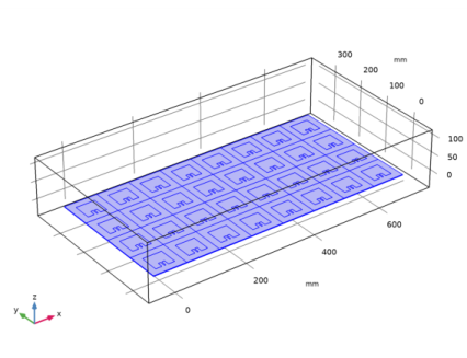
Choose all patch boundaries for the selection.
2
You can do this alternatively by copying the text ’26, 31, 36, 41, 99, 104, 109, 114, 172, 177, 182, 187, 245, 250, 255, 260, 318, 323, 328, 333, 391, 396, 401, 406, 464, 469, 474, 479, 537, 542, 547, 552’, clicking in the selection box, and then pressing Ctrl+V, or by using the Paste Selection dialog box.
Study 1 - Full Array
1
In the Model Builder window, click Study 1.
2
In the Settings window for Study, type Study 1 - Full Array in the Label text field.
Step 1: Frequency Domain
1
In the Model Builder window, under Study 1 - Full Array click Step 1: Frequency Domain.
2
In the Settings window for Frequency Domain, locate the Study Settings section.
3
In the Frequencies text field, type f0.
Parametric Sweep
1
In the Study toolbar, click  Parametric Sweep.
2
In the Settings window for Parametric Sweep, locate the Study Settings section.
3
4
This will simulate when the main beam is normal to the array plane and 30 degrees tilted from the normal axis.
5
In the Study toolbar, click  Compute.
Results
Multislice
1
In the Model Builder window, expand the Results>Electric Field (emw) node.
2
Right-click Multislice and choose Delete.
Electric Field (emw)
1
In the Model Builder window, click Electric Field (emw).
2
In the Settings window for 3D Plot Group, locate the Plot Settings section.
3
Clear the Plot dataset edges check box.
This removes the black geometry edges when plotting the results under this plot group.
Surface 1
1
Right-click Electric Field (emw) and choose Surface.
2
In the Settings window for Surface, locate the Coloring and Style section.
3
From the Color table list, choose JupiterAuroraBorealis.
The Selection subfeature is useful to specify the area of visualization. In this plot, we are interested in visualizing the electric field norm only on the top surface of the antenna substrate (Figure 3).
Selection 1
1
Right-click Surface 1 and choose Selection.
2
In the Settings window for Selection, locate the Selection section.
3
From the Selection list, choose Top surface.
4
In the Electric Field (emw) toolbar, click  Plot.
5
Click the  Zoom Extents button in the Graphics toolbar.
Surface 1
To see the field variation at each column of the array, plot the z-component of the electric field.
1
In the Model Builder window, click Surface 1.
2
In the Settings window for Surface, locate the Expression section.
3
In the Expression text field, type emw.Ez.
4
In the Electric Field (emw) toolbar, click  Plot.
Only the real part is plotted for complex values.
Now, plot the H-plane pattern (Figure 5) of the antenna array by adjusting the default polar plot settings. In this example, the main polarization of the radiated electric field from the microstrip patch antenna is parallel to the y-axis. When plotting the radiation patterns, E- and H-plane are conventionally used. The E-plane is the plane parallel to the antenna main polarization while the H-plane is perpendicular to that polarization. Here, the E-plane is the yz-plane, and the H-plane is the xz-plane.
Radiation Pattern 1
1
In the Model Builder window, expand the Results>2D Far Field (emw) node, then click Radiation Pattern 1.
2
In the Settings window for Radiation Pattern, locate the Expression section.
3
In the Expression text field, type emw.normdBEfar.
4
Locate the Evaluation section. Find the Angles subsection. In the Number of angles text field, type 360.
5
Find the Normal vector subsection. In the y text field, type -1.
6
In the z text field, type 0.
7
In the 2D Far Field (emw) toolbar, click  Plot.
2D Far Field (emw)
1
In the Model Builder window, click 2D Far Field (emw).
2
In the Settings window for Polar Plot Group, locate the Axis section.
3
Select the Manual axis limits check box.
4
In the r minimum text field, type -5.
The minimum level in the polar plot may change the impression on the sidelobe level and beam width.
5
In the 2D Far Field (emw) toolbar, click  Plot.
Radiation Pattern 1
1
In the Model Builder window, expand the Results>3D Far Field (emw) node, then click Radiation Pattern 1.
2
In the Settings window for Radiation Pattern, locate the Expression section.
3
In the Expression text field, type emw.normdBEfar.
4
Select the Threshold check box.
5
6
Locate the Evaluation section. Find the Angles subsection. In the Number of elevation angles text field, type 90.
7
In the Number of azimuth angles text field, type 90.
The higher number of angles results in a finer angular resolution for the 3D far-field pattern.
8
In the 3D Far Field (emw) toolbar, click  Plot.
Simplified Model Using Periodic Conditions
The full array analysis is completed. Build a new model for a simplified analysis using periodic conditions.
Add Component
In the Model Builder window, right-click the root node and choose Add Component>3D.
Geometry 2
1
In the Settings window for Geometry, locate the Units section.
2
From the Length unit list, choose mm.
Add the antenna geometry from the part.
Patch Antenna 1 (pi1)
In the Geometry toolbar, click  Parts and choose Patch Antenna.
Add a block on the top surface of the antenna.
Block 1 (blk1)
1
In the Geometry toolbar, click  Block.
2
In the Settings window for Block, locate the Size and Shape section.
3
In the Width text field, type lda048.
4
In the Depth text field, type lda048.
5
In the Height text field, type 80.
6
Locate the Position section. In the z text field, type 40-d/2.
7
From the Base list, choose Center.
8
Click  Build All Objects.
9
Click the  Wireframe Rendering button in the Graphics toolbar.
10
Click the  Zoom Extents button in the Graphics toolbar.
Add Physics
1
In the Home toolbar, click  Add Physics to open the Add Physics window.
2
Go to the Add Physics window.
3
In the tree, select Radio Frequency>Electromagnetic Waves, Frequency Domain (emw).
4
Find the Physics interfaces in study subsection. In the table, clear the Solve check box for Study 1 - Full Array.
5
Click Add to Component 2 in the window toolbar.
6
In the Home toolbar, click  Add Physics to close the Add Physics window.
Add Study
1
In the Home toolbar, click  Add Study to open the Add Study window.
2
Go to the Add Study window.
3
Find the Studies subsection. In the Select Study tree, select General Studies>Frequency Domain.
4
Find the Physics interfaces in study subsection. In the table, clear the Solve check box for Electromagnetic Waves, Frequency Domain (emw).
5
Click Add Study in the window toolbar.
6
In the Model Builder window, click the root node.
7
In the Home toolbar, click  Add Study to close the Add Study window.
Study 2 - Simplified
In the Settings window for Study, type Study 2 - Simplified in the Label text field.
Step 1: Frequency Domain
1
In the Model Builder window, under Study 2 - Simplified click Step 1: Frequency Domain.
2
In the Settings window for Frequency Domain, locate the Study Settings section.
3
In the Frequencies text field, type f0.
Add a built-in air material for the entire simulation domain and override the antenna substrate with the same dielectric material.
Materials
In the Model Builder window, under Component 2 (comp2) click Materials.
Add Material
1
In the Home toolbar, click  Add Material to open the Add Material window.
2
Go to the Add Material window.
3
4
Click Add to Component in the window toolbar.
5
In the Home toolbar, click  Add Material to close the Add Material window.
Materials
Substrate
1
Right-click Materials and choose Blank Material.
2
In the Settings window for Material, type Substrate in the Label text field.
3
4
Locate the Material Contents section. In the table, enter the following settings:
Electromagnetic Waves, Frequency Domain 2 (emw2)
In the Model Builder window, under Component 2 (comp2) click Electromagnetic Waves, Frequency Domain 2 (emw2).
Lumped Port 1
1
In the Physics toolbar, click  Boundaries and choose Lumped Port.
2
Perfect Electric Conductor 2
1
In the Physics toolbar, click  Boundaries and choose Perfect Electric Conductor.
2
Periodic Condition is the essence of the simplified array design. Assign this boundary condition on each facing pair of all exterior side boundaries.
This mimics an infinite array and the simulation includes the coupling effect with adjacent array elements.
Periodic Condition 1
1
In the Physics toolbar, click  Boundaries and choose Periodic Condition.
2
3
In the Settings window for Periodic Condition, locate the Periodicity Settings section.
4
From the Type of periodicity list, choose Floquet periodicity.
5
Specify the kF vector as
The Floquet periodicity type is useful when defining the phase relation between the source and destination boundaries with an arbitrary angle of incidence. It is characterized by a scaled wave number or a specific wave vector component with respect to the direction from the source to destination boundaries. Here, we assume the radiation through the main beam is dominant in the air domain and its angle is used to configure the k-vector for Floquet periodicity.
Periodic Condition 2
1
In the Physics toolbar, click  Boundaries and choose Periodic Condition.
The beam scanning happens only around the y-axis in the xz-plane. It is assumed that there is no phase variation between the source and destination boundaries normal to the y-axis. The default Continuity type of periodicity is used for those boundaries.
2
Scattering Boundary Condition 1
1
In the Physics toolbar, click  Boundaries and choose Scattering Boundary Condition.
2
Far-Field Domain 1
1
In the Physics toolbar, click  Domains and choose Far-Field Domain.
2
In the Settings window for Far-Field Domain, locate the Domain Selection section.
3
Click  Clear Selection.
4
Note that only the air domain is included in the Far-Field Domain feature. In general, the far-field feature must be applied over the surrounding homogeneous medium. The usage in this example is exceptional by assuming that the radiation can be characterized sufficiently by the near-field in the upper half-space air domain. The current methodology is limited to fast approximation of the antenna array where the major radiation is nether bidirectional nor omnidirectional.
Far-Field Calculation 1
1
In the Model Builder window, expand the Far-Field Domain 1 node, then click Far-Field Calculation 1.
2
In the Settings window for Far-Field Calculation, locate the Boundary Selection section.
3
Click  Clear Selection.
4
Mesh 2
1
In the Model Builder window, under Component 2 (comp2) right-click Mesh 2 and choose Build All.
2
Click the  Click and Hide button in the Graphics toolbar.
3
In the Model Builder window, click Mesh 2.
4
5
6
Click the  Click and Hide button in the Graphics toolbar.
You might have noticed that the shape of the mesh in the specific pair of boundaries in the periodic condition is identical. The mesh sequences set by the Physics-controlled mesh can be reviewed by switching the Sequence type from Physics-controlled mesh to User-controlled mesh, or right-click on the Mesh 2 node in the Model Builder and choose Edit Physics-Induced Sequence.
Study 2 - Simplified
Parametric Sweep
1
In the Study toolbar, click  Parametric Sweep.
2
In the Settings window for Parametric Sweep, locate the Study Settings section.
3
4
5
6
In the Study toolbar, click  Compute.
Results
Electric Field (emw2)
Adjust the default multislice plot settings to see the electric field norm in the substrate.
Multislice
1
In the Model Builder window, expand the Electric Field (emw2) node, then click Multislice.
2
In the Settings window for Multislice, locate the Multiplane Data section.
3
Find the X-planes subsection. In the Planes text field, type 0.
4
Find the Y-planes subsection. In the Planes text field, type 0.
5
Find the Z-planes subsection. From the Entry method list, choose Coordinates.
6
In the Coordinates text field, type 0.
7
In the Electric Field (emw2) toolbar, click  Plot.
2D Far Field (emw2)
The default polar plot is the result of the far-field transformation of a single antenna affected by surrounding array elements. In order to show the radiation pattern (Figure 7) of the 8-by-4 antenna array, the corresponding array factor needs to be multiplied by the single antenna far-field pattern.
1
In the Model Builder window, click 2D Far Field (emw2).
2
In the Settings window for Polar Plot Group, click to expand the Title section.
3
From the Title type list, choose Manual.
4
In the Title text area, type Array Far-Field Comparison (dB).
5
Locate the Axis section. Select the Manual axis limits check box.
6
In the r minimum text field, type -15.
7
In the r maximum text field, type 35.
8
Locate the Legend section. From the Position list, choose Lower right.
Radiation Pattern 1
In dB scale, multiplication is represented by summation. The usage of array factor is discussed in the Model Definition section and also available from Ref. 2.
1
In the Model Builder window, expand the 2D Far Field (emw2) node, then click Radiation Pattern 1.
2
In the Settings window for Radiation Pattern, locate the Expression section.
3
In the Expression text field, type emw2.normdBEfar2++20*log10(emw2.af3(8,4,1,0.48,0.48,0,-2*pi*0.48*cos(phi),0,0)).
4
Locate the Evaluation section. Find the Normal vector subsection. In the y text field, type -1.
5
In the z text field, type 0.
6
Click to expand the Legends section. Select the Show legends check box.
7
From the Legends list, choose Manual.
8
Radiation Pattern 2
1
Right-click Results>2D Far Field (emw2)>Radiation Pattern 1 and choose Duplicate.
2
In the Settings window for Radiation Pattern, locate the Data section.
3
From the Dataset list, choose Study 1 - Full Array/Solution 1 (sol1).
4
Locate the Expression section. In the Expression text field, type emw.normdBEfar.
5
Locate the Legends section. In the table, enter the following settings:
6
Click to expand the Coloring and Style section. Find the Line style subsection. From the Line list, choose Dotted.
7
In the Width text field, type 2.
The comparison in the polar plot shows good agreement good agreement between the full array model and simplified model for the main beam and some sidelobes.
Array Gain Comparison
1
In the Home toolbar, click  Add Plot Group and choose 1D Plot Group.
The radiation pattern can also be plotted in a different format to inspect the level of nulls and sidelobes with a wider plotting dynamic range. Try with 1D plot (Figure 8).
2
In the Settings window for 1D Plot Group, type Array Gain Comparison in the Label text field.
3
Click to expand the Title section. From the Title type list, choose Manual.
4
In the Title text area, type Array Gain Comparison (dBi).
5
Locate the Legend section. From the Position list, choose Lower middle.
Radiation Pattern 1
1
In the Array Gain Comparison toolbar, click  More Plots and choose Radiation Pattern.
2
In the Settings window for Radiation Pattern, locate the Data section.
3
From the Dataset list, choose Study 2 - Simplified/Solution 2 (3) (sol2).
4
Locate the Expression section. In the Expression text field, type emw2.rGaindBEfar+20*log10(emw2.af3(8,4,1,0.48,0.48,0,-2*pi*0.48*cos(phi),0,0))+10*log10(1/32).
5
Locate the Evaluation section. Find the Angles subsection. In the Number of angles text field, type 360.
6
From the Restriction list, choose Manual.
7
In the φ start text field, type -90.
8
Find the Normal vector subsection. In the y text field, type -1.
9
In the z text field, type 0.
10
Click to expand the Legends section. Select the Show legends check box.
11
From the Legends list, choose Manual.
12
13
In the Array Gain Comparison toolbar, click  Plot.
Array Gain Comparison
In the Model Builder window, click Array Gain Comparison.
Radiation Pattern 2
1
In the Array Gain Comparison toolbar, click  More Plots and choose Radiation Pattern.
2
In the Settings window for Radiation Pattern, locate the Data section.
3
From the Dataset list, choose Study 1 - Full Array/Solution 1 (sol1).
4
Locate the Expression section. In the Expression text field, type emw.rGaindBEfar.
5
Locate the Evaluation section. Find the Angles subsection. In the Number of angles text field, type 360.
6
From the Restriction list, choose Manual.
7
In the φ start text field, type -90.
8
Find the Normal vector subsection. In the y text field, type -1.
9
In the z text field, type 0.
10
Click to expand the Coloring and Style section. Find the Line style subsection. From the Line list, choose Dashed.
11
Find the Line markers subsection. From the Marker list, choose Cycle.
12
In the Number text field, type 31.
13
Locate the Legends section. Select the Show legends check box.
14
From the Legends list, choose Manual.
15
16
In the Array Gain Comparison toolbar, click  Plot.