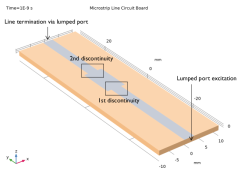
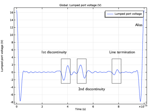
PDF

Study of a Defective Microstrip Line via Frequency-to-Time FFT Analysis
Introduction
While transient analyses are useful for time domain reflectometry (TDR) to handle signal integrity (SI) problems, many RF and microwave examples are addressed using frequency domain simulations generating S-parameters. However, from the frequency domain data it is difficult to identify sources for this signal degradation.
This example simulates a microstrip line in frequency domain with a couple of line width discontinuities and performs frequency-to-time fast Fourier transform. The computed results help to identify the physical discontinuities and impedance mismatches on the transmission line, by analyzing the signal fluctuation in the time domain.
Figure 1: Microstrip line circuit board model using lumped ports. The surrounding air domain is not included for visualization purposes.
Model Definition
The model describes a 50 Ω microstrip line on a 60 mil substrate with the dielectric constant of εr = 3.38. A wider strip is placed in the middle of the microstrip line to represent a lower impedance line causing unwanted reflections. All metallic parts, including the patterned line on the top of the substrate and bottom ground plane, are set to perfect electric conductor (PEC) by ignoring the loss from a finite conductivity to simplify the modeling process. The small rectangular surfaces, bridging between each microstrip end and the ground plane, are used to add lumped ports. The lumped ports excite the microstrip line and terminate it with 50 Ω characteristic impedance. The material on top of the circuit board is air. The exterior surfaces of the air are finished by a scattering boundary condition that is an absorbing boundary to describe an open radiating space.
The study consists of two steps:
The time domain results may vary with the input arguments in each study step.
The frequency step, Δf, is set to make the period of alias in the time domain response greater than the round trip travel time from the excitation, lumped port 1, to the line termination, lumped port 2:
1/Df = 1 ns > 65 mm/c_const*sqrt(3.38)*2 = 0.7.9723 ns
where 65 mm is the circuit board length and c_const is a predefined COMSOL constant for the speed of light in vacuum.
While performing FFT, a Gaussian window function is used. This helps to suppress the noise coming from the limited range of the frequency sweep. Each study step uses “Store fields in output” that defines the selections where the computed results are stored. By choosing only the lumped port boundaries for Store fields in output settings, it is possible to reduce the size of the model file a lot.
Results and Discussion
Figure 2 shows the electric field norm on the lumped port boundaries in the time domain. The boundaries include the solutions transformed from the frequency-domain data. Since the FFT only transforms the dependent variable, the electric field E, to the time domain, it is only possible to use postprocessing variables directly related to E in the time domain. The frequency domain response is still accessible through Solution Store 1 dataset.
Figure 2: Time domain field on the lumped port boundaries.
Figure 3: Time domain lumped port voltage. The overshoot and undershoot of the signal indicate the discontinuities of the microstrip line.
In Figure 3, the time domain results of the voltage bandpass impulse response at lumped port 1 is plotted. The voltage fluctuation times correspond to the propagation times for the incident pulse to be reflected from the two line discontinuities-the defective parts of the 50 Ω microstrip line. The round trip travel time from lumped port 1 to each discontinuity is described in Table 2 below. The estimated time agrees with the voltage fluctuation location in Figure 3.
The alias of the FFT is observed at 1 ns that is the inverse of the frequency step used in the frequency domain study step.
Notes About the COMSOL Implementation
The frequency-to-time fast Fourier transform (FFT) study step transforms the solution of dependent variables in frequency domain to time domain with a very small time step, ten samples per period, defined by the highest frequency in this model. Only the postprocessing variables that can be expressed with the dependent variables are valid for result analysis. Since the transformed solutions typically contain many time steps, it is recommended to use the Store field in output option to reduce the size of the model.
Application Library path: RF_Module/EMI_EMC_Applications/microstrip_line_discontinuity
Modeling Instructions
From the File menu, choose New.
New
In the New window, click  Model Wizard.
Model Wizard
1
In the Model Wizard window, click  3D.
2
In the Select Physics tree, select Radio Frequency>Electromagnetic Waves, Frequency Domain (emw).
3
Click Add.
4
Click  Study.
5
In the Select Study tree, select General Studies>Frequency Domain.
6
Global Definitions
Parameters 1
1
In the Model Builder window, under Global Definitions click Parameters 1.
2
In the Settings window for Parameters, locate the Parameters section.
3
Study 1
Step 1: Frequency Domain
1
In the Model Builder window, under Study 1 click Step 1: Frequency Domain.
2
In the Settings window for Frequency Domain, locate the Study Settings section.
3
In the Frequencies text field, type range(0.001[GHz],df,2*f0).
Geometry 1
1
In the Model Builder window, under Component 1 (comp1) click Geometry 1.
2
In the Settings window for Geometry, locate the Units section.
3
From the Length unit list, choose mm.
Block 1 (blk1)
1
In the Geometry toolbar, click  Block.
2
In the Settings window for Block, locate the Size and Shape section.
3
In the Width text field, type 20.
4
In the Depth text field, type 65.
5
In the Height text field, type 1.524.
6
Locate the Position section. From the Base list, choose Center.
Create a block for the microstrip line trace and two lumped port boundaries.
Block 2 (blk2)
1
In the Geometry toolbar, click  Block.
2
In the Settings window for Block, locate the Size and Shape section.
3
In the Width text field, type 3.3.
4
In the Depth text field, type 65.
5
In the Height text field, type 1.524.
6
Locate the Position section. From the Base list, choose Center.
Block 3 (blk3)
1
In the Geometry toolbar, click  Block.
2
In the Settings window for Block, locate the Size and Shape section.
3
In the Width text field, type 30.
4
In the Depth text field, type 70.
5
In the Height text field, type 10.
6
Locate the Position section. In the z text field, type (10-1.524)/2.
7
From the Base list, choose Center.
8
Click  Build Selected.
9
Click  Build Selected.
10
Click the  Wireframe Rendering button in the Graphics toolbar.
Work Plane 1 (wp1)
1
In the Geometry toolbar, click  Work Plane.
2
In the Settings window for Work Plane, locate the Plane Definition section.
3
From the Plane type list, choose Face parallel.
4
On the object blk1, select Boundary 4 only.
It might be easier to select the correct boundary by using the Selection List window. To open this window, in the Home toolbar click Windows and choose Selection List. (If you are running the cross-platform desktop, you find Windows in the main menu.)
Work Plane 1 (wp1)>Plane Geometry
In the Model Builder window, click Plane Geometry.
Work Plane 1 (wp1)>Rectangle 1 (r1)
1
In the Work Plane toolbar, click  Rectangle.
2
In the Settings window for Rectangle, locate the Size and Shape section.
3
In the Width text field, type 6.
4
In the Height text field, type 11.
5
Locate the Position section. In the xw text field, type -3.
6
In the yw text field, type -10.
7
In the Model Builder window, right-click Geometry 1 and choose Build All.
Electromagnetic Waves, Frequency Domain (emw)
Lumped Port 1
1
In the Model Builder window, under Component 1 (comp1) right-click Electromagnetic Waves, Frequency Domain (emw) and choose Lumped Port.
2
3
In the Settings window for Lumped Port, locate the Boundary Selection section.
4
Click  Create Selection.
5
In the Create Selection dialog box, click OK.
Lumped Port 2
1
In the Physics toolbar, click  Boundaries and choose Lumped Port.
2
3
In the Settings window for Lumped Port, locate the Boundary Selection section.
4
Click  Create Selection.
The added selection will be used to define where to store the results. The model evaluates only the lumped port voltage in time and frequency domain.
5
In the Create Selection dialog box, click OK.
Perfect Electric Conductor 2
1
In the Physics toolbar, click  Boundaries and choose Perfect Electric Conductor.
2
Scattering Boundary Condition 1
1
In the Physics toolbar, click  Boundaries and choose Scattering Boundary Condition.
2
Add Material
1
In the Home toolbar, click  Add Material to open the Add Material window.
2
Go to the Add Material window.
3
4
Click Add to Component in the window toolbar.
5
In the Home toolbar, click  Add Material to close the Add Material window.
Materials
Material 2 (mat2)
1
In the Model Builder window, under Component 1 (comp1) right-click Materials and choose Blank Material.
2
3
In the Settings window for Material, locate the Material Contents section.
4
Mesh 1
1
In the Model Builder window, under Component 1 (comp1) right-click Mesh 1 and choose Build All.
2
Click the  Click and Hide button in the Graphics toolbar.
3
4
5
Study 1
Step 1: Frequency Domain
The period of a ripple noise and alias after FFT are defined by the inverse of the maximum frequency and frequency step, respectively.
1
In the Model Builder window, under Study 1 click Step 1: Frequency Domain.
2
In the Settings window for Frequency Domain, click to expand the Values of Dependent Variables section.
3
Find the Store fields in output subsection. From the Settings list, choose For selections.
4
Under Selections, click  Add.
5
In the Add dialog box, in the Selections list, choose Explicit 1 and Explicit 2.
6
By choosing only the port boundaries for Store fields in output settings, it is possible to reduce the size of a model file a lot. The lumped port boundaries are included for the voltage evaluation.
Frequency to Time FFT
1
In the Study toolbar, click  Study Steps and choose Time Dependent>Frequency to Time FFT.
2
In the Settings window for Frequency to Time FFT, locate the Study Settings section.
3
In the Times text field, type range(0,1/f0/20,1/df).
4
From the Scaling list, choose Discrete Fourier transform.
Use Window function to suppress a high frequency ripple noise.
5
Select the Use window function check box.
6
From the Window function list, choose Gaussian.
7
In the Window center text field, type f0.
8
In the Standard deviation text field, type f0/4.
9
Click to expand the Values of Dependent Variables section. Find the Store fields in output subsection. From the Settings list, choose For selections.
10
Under Selections, click  Add.
11
In the Add dialog box, in the Selections list, choose Explicit 1 and Explicit 2.
12
13
In the Study toolbar, click  Compute.
Results
Multislice
1
In the Model Builder window, expand the Electric Field (emw) node.
2
Right-click Multislice and choose Delete.
Surface 1
In the Model Builder window, right-click Electric Field (emw) and choose Surface.
Selection 1
1
In the Model Builder window, right-click Surface 1 and choose Selection.
2
3
In the Electric Field (emw) toolbar, click  Plot.
The results only on the lumped port boundaries are evaluated.
1D Plot Group 2
In the Home toolbar, click  Add Plot Group and choose 1D Plot Group.
Global 1
1
Right-click 1D Plot Group 2 and choose Global.
2
In the Settings window for Global, locate the y-Axis Data section.
3
4
In the 1D Plot Group 2 toolbar, click  Plot.
Compare the reproduced plot with Figure 2.
A simple microstrip line circuit board can be visualized for presentation purposes without using the computed results.
Circuit board
1
In the Home toolbar, click  Add Plot Group and choose 3D Plot Group.
2
In the Settings window for 3D Plot Group, type Circuit board in the Label text field.
3
Click to expand the Title section. From the Title type list, choose Manual.
4
In the Title text area, type Microstrip Line Circuit Board.
Surface 1
1
Right-click Circuit board and choose Surface.
2
In the Settings window for Surface, locate the Expression section.
3
In the Expression text field, type 1.
4
Locate the Coloring and Style section. From the Coloring list, choose Uniform.
5
From the Color list, choose Custom.
6
7
Click Define custom colors.
8
9
Click Add to custom colors.
10
Click Show color palette only or OK on the cross-platform desktop.
Selection 1
1
Right-click Surface 1 and choose Selection.
2
Surface 2
1
In the Model Builder window, right-click Circuit board and choose Surface.
2
In the Settings window for Surface, locate the Expression section.
3
In the Expression text field, type 1.
4
Locate the Coloring and Style section. From the Coloring list, choose Uniform.
5
From the Color list, choose Custom.
6
7
Click Define custom colors.
8
9
Click Add to custom colors.
10
Click Show color palette only or OK on the cross-platform desktop.
Selection 1
1
Right-click Surface 2 and choose Selection.
2
3
In the Circuit board toolbar, click  Plot.
Circuit board
1
In the Model Builder window, click Circuit board.
2
In the Settings window for 3D Plot Group, locate the Plot Settings section.
3
Clear the Plot dataset edges check box.
4
In the Circuit board toolbar, click  Plot.