PDF

A Low-Pass and Band-Pass Filter Using Lumped Elements
Introduction
Passive devices can be designed using lumped element features if both the operating frequency of the device and the insertion loss of lumped elements are low. This example simulates two types of lumped element filters. First, a 5-element maximally flat low-pass filter is built to compute frequency responses that show the cutoff at the intended frequency. Second, a band-pass filter transformed from the low-pass filter design is simulated in the same frequency range. Both filter models present S-parameters and electric field distribution by default.
Figure 1: 0402 surface-mount device (SMD) inductors and capacitors are modeled using lumped element features on 2D boundaries. The figure describes only a low-pass filter model.
Model Definition
This example shows a filter design with five SMD devices soldered to a microstrip line that sits on a 60 mil substrate with a ground plane (Figure 1). The performance of each SMD device is assumed to be ideal in the simulated frequency range. All metal parts the microstrip line, the thin copper ground plane and the metalized via holes are modeled as perfect electric conductors (PECs). Each end of the microstrip line is configured with a lumped port. One of the lumped ports is the source for the input signal.
The geometry of each SMD device is simplified as a 2D boundary and the electrical performance is modeled using a lumped element. Lumped elements are similar to lumped ports except that they are strictly passive and there are predefined choices for inductances and capacitance.
The dielectric constant of the substrate is εr = 3.38 and the remaining volume in the model is air. The device is assumed to sit in open space, and thus the air domain is truncated using the scattering boundary condition to absorb radiation from the circuit.
Low-Pass Filter
The filter in this example consists of inductors connected in series and capacitors connected in parallel. The capacitors are connected to a small section of microstrip line that is, in turn, connected to the metal vias shorted to the ground plane. The element values either L or C of the desired filter are defined by
The calculated values are shown in Table 1.
g1
g2
g3
g4
g5
g6
These values are determined assuming that the reference impedance is 1 Ω and the cutoff frequency of the filter is 1 Hz. However, for the particular filter in the model, the reference impedance is 50 Ω and the cutoff frequency is 1 GHz. The filter element values, L and C, are scaled using the equations below, where R0 is reference impedance and fc is cutoff frequency of the filter.
,
The resulting scaled element values are L1 = L3 = 4.9179 nH, L2 = 15.915 nH and C1 = C2 = 5.1503 pF.
Band-Pass Filter
The low-pass filter can be converted to a band-pass filter by transforming series inductors (L) and parallel capacitors (C) to a series LC and a parallel LC circuit, respectively. The value of transformed lumped elements are scaled by impedance and frequency based on the element values for the low pass filter prototype (Table 1).
In a series LC circuit,
,
In a parallel LC circuit,
,
where fc is used for the center frequency of the filter and Δ is the fractional bandwidth defined as bandwidth/fc.
Results and Discussion
The norm of the electric field underneath the microstrip lines at 2 GHz is plotted in Figure 2. This frequency is outside the passband of the filter and the plot illustrates that the signal is blocked. In Figure 3, the norm of the field is plotted at 0.3 GHz, which is within the passband of the filter. The plot shows that the wave propagates through the filter.
Figure 2: The norm of the electric field at 2 GHz, which is outside the passband of the filter, shows that the energy from the input port cannot reach the output port.
Figure 3: The norm of the electric field is plotted at 0.3 GHz, which is within the passband of the filter. The SMD filter lets the signal pass from the input port to the output port.
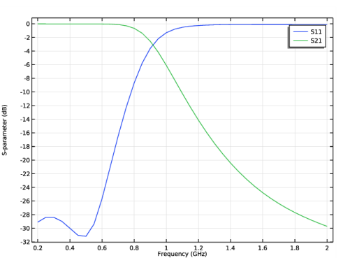
The calculated S-parameters, plotted in Figure 4, show a low-pass filter frequency response with 1 GHz cutoff frequency. A small frequency shift is observed due to the parasitic reactance caused by the metal pads and via holes connecting the SMD devices to the ground plane.
Figure 4: The S-parameters are plotted as a function of frequency to illustrate the filter response. The cutoff frequency of the low-pass filter is observed near 1 GHz.
Figure 5: The norm of the electric field at 2 GHz, which is outside the passband of the filter, shows that the energy from the input port cannot reach the output port.
Figure 6: The norm of the electric field is plotted at 1 GHz, which is within the passband of the filter. The SMD filter lets the signal pass from the input port to the output port.
Figure 7: The S-parameter plot illustrates the frequency response of the band-pass filter. The center frequency is observed at 1 GHz.
The S-parameters of the band-pass filter are plotted in Figure 7. Due to the parasitic reactance from the metal pads and via holes, the frequency responses outside the passband are not ideal as those obtained from a circuit theory.
Reference
1. D.M. Pozar, Microwave Engineering, John Wiley & Sons, 1998.
2. R.E. Collin, Foundation of Microwave Engineering, McGraw-Hill, 1992.
Application Library path: RF_Module/Filters/lumped_element_filter
Modeling Instructions
From the File menu, choose New.
New
In the New window, click  Model Wizard.
Model Wizard
1
In the Model Wizard window, click  3D.
2
In the Select Physics tree, select Radio Frequency>Electromagnetic Waves, Frequency Domain (emw).
3
Click Add.
4
Click  Study.
5
In the Select Study tree, select General Studies>Frequency Domain.
6
Study 1
Step 1: Frequency Domain
1
In the Model Builder window, under Study 1 click Step 1: Frequency Domain.
2
In the Settings window for Frequency Domain, locate the Study Settings section.
3
In the Frequencies text field, type range(0.2[GHz],0.05[GHz],2[GHz]).
Global Definitions
Parameters 1
1
In the Model Builder window, under Global Definitions click Parameters 1.
2
In the Settings window for Parameters, locate the Parameters section.
3
50 Ω
Here, mil refers to the unit milliinch.
Geometry 1
1
In the Model Builder window, under Component 1 (comp1) click Geometry 1.
2
In the Settings window for Geometry, locate the Units section.
3
From the Length unit list, choose mm.
Block 1 (blk1)
1
In the Geometry toolbar, click  Block.
2
In the Settings window for Block, locate the Size and Shape section.
3
In the Width text field, type 16.
4
In the Depth text field, type 37.5.
5
In the Height text field, type 8.
6
Locate the Position section. From the Base list, choose Center.
7
Click  Build Selected.
8
Click the  Wireframe Rendering button in the Graphics toolbar.
Block 2 (blk2)
1
In the Geometry toolbar, click  Block.
2
In the Settings window for Block, locate the Size and Shape section.
3
In the Width text field, type 16.
4
In the Depth text field, type 30.
5
In the Height text field, type thickness.
6
Locate the Position section. From the Base list, choose Center.
7
In the z text field, type -4+thickness/2.
Block 3 (blk3)
1
In the Geometry toolbar, click  Block.
2
In the Settings window for Block, locate the Size and Shape section.
3
In the Width text field, type 3.2.
4
In the Depth text field, type 11.9.
5
In the Height text field, type thickness.
6
Locate the Position section. From the Base list, choose Center.
7
In the y text field, type 9.05.
8
In the z text field, type -4+thickness/2.
Mirror 1 (mir1)
1
In the Geometry toolbar, click  Transforms and choose Mirror.
2
3
In the Settings window for Mirror, locate the Input section.
4
Select the Keep input objects check box.
5
Locate the Normal Vector to Plane of Reflection section. In the y text field, type -1.
6
In the z text field, type 0.
Work Plane 1 (wp1)
1
In the Geometry toolbar, click  Work Plane.
2
In the Settings window for Work Plane, locate the Plane Definition section.
3
In the z-coordinate text field, type -4+thickness.
4
Click  Show Work Plane.
Work Plane 1 (wp1)>Rectangle 1 (r1)
1
In the Work Plane toolbar, click  Rectangle.
2
In the Settings window for Rectangle, locate the Size and Shape section.
3
In the Width text field, type 0.5.
4
In the Height text field, type 3.6.
5
Locate the Position section. From the Base list, choose Center.
6
In the yw text field, type 1.3.
7
Click to expand the Layers section. In the table, enter the following settings:
8
Select the Layers on top check box.
Work Plane 1 (wp1)>Rectangle 2 (r2)
1
In the Work Plane toolbar, click  Rectangle.
2
In the Settings window for Rectangle, locate the Size and Shape section.
3
In the Height text field, type 0.5.
4
Locate the Position section. From the Base list, choose Center.
5
In the xw text field, type -0.75.
6
In the yw text field, type 1.3.
Work Plane 1 (wp1)>Mirror 1 (mir1)
1
In the Work Plane toolbar, click  Transforms and choose Mirror.
2
Click in the Graphics window and then press Ctrl+A to select both objects.
3
In the Settings window for Mirror, locate the Input section.
4
Select the Keep input objects check box.
5
Locate the Normal Vector to Line of Reflection section. In the xw text field, type 0.
6
In the yw text field, type 1.
7
Click  Build Selected.
Work Plane 1 (wp1)>Rectangle 3 (r3)
1
In the Work Plane toolbar, click  Rectangle.
2
In the Settings window for Rectangle, locate the Position section.
3
In the xw text field, type -3.25.
4
In the yw text field, type -2.3.
5
Locate the Size and Shape section. In the Width text field, type 2.
6
In the Height text field, type 4.6.
Cylinder 1 (cyl1)
1
In the Model Builder window, right-click Geometry 1 and choose Cylinder.
2
In the Settings window for Cylinder, locate the Size and Shape section.
3
In the Radius text field, type 0.4.
4
In the Height text field, type thickness.
5
Locate the Position section. In the x text field, type -2.25.
6
In the y text field, type -1.5.
7
In the z text field, type -4.
Array 1 (arr1)
1
In the Geometry toolbar, click  Transforms and choose Array.
2
3
In the Settings window for Array, locate the Size section.
4
In the y size text field, type 3.
5
Locate the Displacement section. In the y text field, type 1.5.
6
Click  Build All Objects.
The finished geometry should look like this.
Set up the physics. Use lumped ports for the S-parameter analysis and lumped elements to model the SMD devices.
Electromagnetic Waves, Frequency Domain (emw)
1
In the Model Builder window, under Component 1 (comp1) click Electromagnetic Waves, Frequency Domain (emw).
2
Perfect Electric Conductor 2
1
In the Physics toolbar, click  Boundaries and choose Perfect Electric Conductor.
2
You can do this most easily by copying the text ’7, 12, 33, 34, 38, 39, 45, and 47’, clicking in the selection box, and then pressing Ctrl+V, or by using the Paste Selection dialog box
Lumped Port 1
1
In the Physics toolbar, click  Boundaries and choose Lumped Port.
2
For the first port, wave excitation is on by default.
Lumped Port 2
1
In the Physics toolbar, click  Boundaries and choose Lumped Port.
2
Lumped Element 1
1
In the Physics toolbar, click  Boundaries and choose Lumped Element.
2
3
In the Settings window for Lumped Element, locate the Settings section.
4
From the Lumped element device list, choose Inductor.
5
In the Lelement text field, type l1.
Lumped Element 2
1
In the Physics toolbar, click  Boundaries and choose Lumped Element.
2
3
In the Settings window for Lumped Element, locate the Settings section.
4
From the Lumped element device list, choose Inductor.
5
In the Lelement text field, type l2.
Lumped Element 3
1
In the Physics toolbar, click  Boundaries and choose Lumped Element.
2
3
In the Settings window for Lumped Element, locate the Settings section.
4
From the Lumped element device list, choose Inductor.
5
In the Lelement text field, type l1.
Lumped Element 4
1
In the Physics toolbar, click  Boundaries and choose Lumped Element.
2
3
In the Settings window for Lumped Element, locate the Settings section.
4
From the Lumped element device list, choose Capacitor.
5
In the Celement text field, type c1.
Lumped Element 5
1
In the Physics toolbar, click  Boundaries and choose Lumped Element.
2
3
In the Settings window for Lumped Element, locate the Settings section.
4
From the Lumped element device list, choose Capacitor.
5
In the Celement text field, type c1.
Scattering Boundary Condition 1
1
In the Physics toolbar, click  Boundaries and choose Scattering Boundary Condition.
2
Add Material
1
In the Home toolbar, click  Add Material to open the Add Material window.
2
Go to the Add Material window.
3
4
Click Add to Component in the window toolbar.
5
In the Home toolbar, click  Add Material to close the Add Material window.
Materials
Material 2 (mat2)
1
In the Model Builder window, under Component 1 (comp1) right-click Materials and choose Blank Material.
2
3
In the Settings window for Material, locate the Material Contents section.
4
Mesh 1
In the Model Builder window, under Component 1 (comp1) right-click Mesh 1 and choose Build All.
Definitions
Hide for Physics 1
1
In the Model Builder window, expand the Component 1 (comp1)>Definitions node.
2
Right-click View 1 and choose Hide for Physics.
3
In the Settings window for Hide for Physics, locate the Geometric Entity Selection section.
4
From the Geometric entity level list, choose Boundary.
5
Mesh 1
In the Model Builder window, click Mesh 1.
The meshed structure should look like this figure.
Study 1
In the Home toolbar, click  Compute.
Results
Multislice
Modify the settings to show the plot only on the xy-plane.
1
In the Model Builder window, expand the Electric Field (emw) node, then click Multislice.
2
In the Settings window for Multislice, locate the Multiplane Data section.
3
Find the X-planes subsection. In the Planes text field, type 0.
4
Find the Y-planes subsection. In the Planes text field, type 0.
5
Find the Z-planes subsection. From the Entry method list, choose Coordinates.
6
In the Coordinates text field, type -4+thickness/2.
7
In the Electric Field (emw) toolbar, click  Plot.
This reproduces Figure 2 showing the electric field distribution outside the passband.
Electric Field (emw)
1
In the Model Builder window, click Electric Field (emw).
2
In the Settings window for 3D Plot Group, locate the Data section.
3
From the Parameter value (freq (GHz)) list, choose 0.3.
4
In the Electric Field (emw) toolbar, click  Plot.
Compare the reproduced plot with Figure 3 showing the electric field distribution inside the passband.
S-parameter (emw)
This shows the frequency response of the low-pass filter. See Figure 4.
Smith Plot (emw)
Global Definitions
Parameters 1
1
In the Model Builder window, under Global Definitions click Parameters 1.
2
In the Settings window for Parameters, locate the Parameters section.
3
Electromagnetic Waves, Frequency Domain (emw)
Lumped Element 1
1
In the Model Builder window, expand the Component 1 (comp1)>Electromagnetic Waves, Frequency Domain (emw)>Lumped Element 1 node, then click Lumped Element 1.
2
In the Settings window for Lumped Element, locate the Settings section.
3
From the Lumped element device list, choose Series LC.
4
In the Lelement text field, type l1_inductor.
5
In the Celement text field, type l1_capacitor.
Lumped Element 2
1
In the Model Builder window, click Lumped Element 2.
2
In the Settings window for Lumped Element, locate the Settings section.
3
From the Lumped element device list, choose Series LC.
4
In the Lelement text field, type l2_inductor.
5
In the Celement text field, type l2_capacitor.
Lumped Element 3
1
In the Model Builder window, click Lumped Element 3.
2
In the Settings window for Lumped Element, locate the Settings section.
3
From the Lumped element device list, choose Series LC.
4
In the Lelement text field, type l1_inductor.
5
In the Celement text field, type l1_capacitor.
Lumped Element 4
1
In the Model Builder window, click Lumped Element 4.
2
In the Settings window for Lumped Element, locate the Settings section.
3
From the Lumped element device list, choose Parallel LC.
4
In the Lelement text field, type c1_inductor.
5
In the Celement text field, type c1_capacitor.
Lumped Element 5
1
In the Model Builder window, click Lumped Element 5.
2
In the Settings window for Lumped Element, locate the Settings section.
3
From the Lumped element device list, choose Parallel LC.
4
In the Lelement text field, type c1_inductor.
5
In the Celement text field, type c1_capacitor.
Add Study
1
In the Home toolbar, click  Add Study to open the Add Study window.
2
Go to the Add Study window.
3
Find the Studies subsection. In the Select Study tree, select General Studies>Frequency Domain.
4
Click Add Study in the window toolbar.
5
In the Home toolbar, click  Add Study to close the Add Study window.
Study 2
Step 1: Frequency Domain
1
In the Settings window for Frequency Domain, locate the Study Settings section.
2
In the Frequencies text field, type range(0.2[GHz],0.05[GHz],2[GHz]).
3
In the Home toolbar, click  Compute.
Results
Multislice
Modify the settings to show the plot only on the xy-plane.
1
In the Model Builder window, expand the Electric Field (emw) 1 node, then click Multislice.
2
In the Settings window for Multislice, locate the Multiplane Data section.
3
Find the X-planes subsection. In the Planes text field, type 0.
4
Find the Y-planes subsection. In the Planes text field, type 0.
5
Find the Z-planes subsection. From the Entry method list, choose Coordinates.
6
In the Coordinates text field, type -4+thickness/2.
7
In the Electric Field (emw) 1 toolbar, click  Plot.
This reproduces Figure 5 showing the electric field distribution outside the passband.
Electric Field (emw) 1
1
In the Model Builder window, click Electric Field (emw) 1.
2
In the Settings window for 3D Plot Group, locate the Data section.
3
From the Parameter value (freq (GHz)) list, choose 1.
4
In the Electric Field (emw) 1 toolbar, click  Plot.
Compare the reproduced plot with Figure 6 showing the electric field distribution inside the passband.
S-parameter (emw) 1
The frequency response (S-parameters) is shown in Figure 7.
Smith Plot (emw) 1
Analyze the same bandpass filter model with a much finer frequency resolution using Adaptive Frequency Sweep based on asymptotic waveform evaluation (AWE). When a device presents a slowly varying frequency response, the AWE method provides a faster solution time when running the simulation on many frequency points. The following example with the Adaptive Frequency Sweep can be computed about twenty times faster than regular Frequency Domain sweeps with a same finer frequency resolution.
Electromagnetic Waves, Frequency Domain (emw)
Lumped Port 1
1
In the Model Builder window, under Component 1 (comp1)>Electromagnetic Waves, Frequency Domain (emw) click Lumped Port 1.
2
In the Settings window for Lumped Port, locate the Boundary Selection section.
3
Click  Create Selection.
4
In the Create Selection dialog box, type Lumped port 1 in the Selection name text field.
5
Lumped Port 2
1
In the Model Builder window, click Lumped Port 2.
2
In the Settings window for Lumped Port, locate the Boundary Selection section.
3
Click  Create Selection.
4
In the Create Selection dialog box, type Lumped port 2 in the Selection name text field.
5
Add Study
1
In the Home toolbar, click  Add Study to open the Add Study window.
2
Go to the Add Study window.
3
Find the Studies subsection. In the Select Study tree, select Preset Studies for Selected Physics Interfaces>Adaptive Frequency Sweep.
4
Click Add Study in the window toolbar.
5
In the Home toolbar, click  Add Study to close the Add Study window.
Study 3
Step 1: Adaptive Frequency Sweep
1
In the Settings window for Adaptive Frequency Sweep, locate the Study Settings section.
2
In the Frequencies text field, type range(0.2[GHz],0.001[GHz],2[GHz]).
Use a 50 times finer frequency resolution.
A slowly varying scalar value curve works well for AWE expressions. When AWE expression type is set to Physics controlled in the Adaptive Frequency Sweep study settings, abs(comp1.emw.S21) is used automatically for two-port devices.
Because such a fine frequency step generates a memory-intensive solution, the model file size will increase tremendously when it is saved. When only the frequency response of port related variables are of interest, it is not necessary to store all of the field solutions. By selecting the Store fields in output check box in the Values of Dependent Variables section, we can control the part of the model on which the computed solution is saved. We only add the selection containing these boundaries where the port variables are calculated. The lumped port size is typically very small compared to the entire modeling domain, and the saved file size with the fine frequency step is more or less that of the regular discrete frequency sweep model when only the solutions on the port boundaries are stored.
3
Locate the Values of Dependent Variables section. Find the Store fields in output subsection. From the Settings list, choose For selections.
4
Under Selections, click  Add.
5
In the Add dialog box, in the Selections list, choose Lumped port 1 and Lumped port 2.
6
It is necessary to include the lumped port boundaries to calculate S-parameters. By choosing only the lumped port boundaries for Store fields in output settings, it is possible to reduce the size of a model file a lot.
7
In the Home toolbar, click  Compute.
Results
Multislice
1
In the Model Builder window, expand the Electric Field (emw) 2 node.
2
Right-click Multislice and choose Delete.
Surface 1
In the Model Builder window, right-click Electric Field (emw) 2 and choose Surface.
Selection 1
1
In the Model Builder window, right-click Surface 1 and choose Selection.
2
3
In the Electric Field (emw) 2 toolbar, click  Plot.
S-parameter (emw) 2
1
In the Model Builder window, click S-parameter (emw) 2.
2
In the Settings window for 1D Plot Group, locate the Legend section.
3
From the Position list, choose Lower right.
Global 1
1
In the Model Builder window, expand the S-parameter (emw) 2 node, then click Global 1.
2
In the Settings window for Global, locate the y-Axis Data section.
3
Global 2
1
Right-click Results>S-parameter (emw) 2>Global 1 and choose Duplicate.
2
In the Settings window for Global, locate the Data section.
3
From the Dataset list, choose Study 2/Solution 2 (sol2).
4
Locate the y-Axis Data section. In the table, enter the following settings:
5
Click to expand the Coloring and Style section. Find the Line style subsection. From the Line list, choose Cycle.
6
Find the Line markers subsection. From the Marker list, choose Cycle.
7
From the Positioning list, choose In data points.
8
In the S-parameter (emw) 2 toolbar, click  Plot.