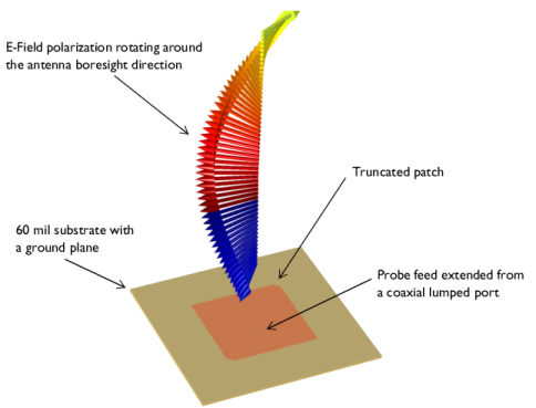
PDF

Circularly Polarized Antenna for GPS Applications
Introduction
One way to generate circular polarization from a microstrip patch antenna is to truncate the patch radiator. This example is tuned around the GPS frequency range. The axial ratios are calculated to show the degree of circular polarization.
Figure 1: A truncated microstrip patch antenna fed by a probe generates circular polarization along the main radiation direction. Perfectly matched layers enclosing the model domain are not shown in this figure.
Model Definition
A circularly polarized microstrip patch antenna design begins by adding a square metallic patch on top of a 60 mil substrate with a ground plane. The patch size is approximately estimated by a half wavelength inside the substrate;
where c0 is the speed of light, f0 is frequency, and εr is the relative permittivity of a substrate. This estimated value is only an initial guess number and the size needs to be tuned precisely for the intended frequency.
The basic square or rectangular patch radiator generates a linear polarization. By truncating two diagonally paired corners of the patch, the antenna can produce a circular polarization; electric fields with a fairly equal magnitude and ~90 degree phase difference between two orthogonal components; x- and y-axis field components.
A rigid coaxial cable filled with Teflon (εr = 2.1) is added on the bottom of the substrate and the outer conductor of the coaxial cable is connected to the ground plane. The inner conductor pin of the cable is extended through the dielectric part of the substrate and shorted to the patch on the top surface. All metal parts including the patch, ground plane, inner and outer conductors of the coaxial cable are modeled as perfect electric conductors.
A coaxial lumped port is used to excite the antenna. It is known that the input impedance on the edge center of a patch is very high while the input impedance around the center of the patch is quite low. The port location is optimized between these two points to get the best matching to the reference impedance 50 Ω with a coaxial probe feed.
The antenna is modeled in a spherical air domain. The air domain is truncated with Perfectly Matched Layers (PMLs) which absorb all outgoing radiation.
All domains except the PMLs are meshed by a tetrahedral mesh with maximum element size of five elements per wavelength so that the wave is well-resolved. The parts in the coaxial cable are meshed more finely to provide good resolution of the curved surfaces. The PMLs are swept with a total of five elements along the absorbing direction.
Results and Discussion
The default plot is modified to show the electric fields only on xy-plane (Figure 2). In general, a linearly polarized patch antenna provides strong fields on two parallel radiating edges. However, the truncated patch antenna shows the radiating fields confined at each corner of the patch. The antenna performs almost equally at every azimuthal angle in terms of the field intensity magnitude.
The axial ratio, which is a measure of the circularity of the polarization, is plotted in Figure 3. In the positive z direction, the evaluated value is less than 3 dB.
The 3D far-field radiation pattern is shown in Figure 4. Because the size of the ground plane is bigger than that of the radiating patch, it blocks the backward radiation and make the pattern directive in the positive z direction.
Figure 2: All corners are excited almost equally. This condition is necessary for the antenna to create a circular polarization.
Figure 3: The minimum axial ratio is observed at the antenna boresight (the positive z direction).
Figure 4: The 3D far-field pattern is directed to the positive z direction due to the ground plane.
Application Library path: RF_Module/Antennas/circularly_polarized_antenna
Modeling Instructions
From the File menu, choose New.
New
In the New window, click  Model Wizard.
Model Wizard
1
In the Model Wizard window, click  3D.
2
In the Select Physics tree, select Radio Frequency>Electromagnetic Waves, Frequency Domain (emw).
3
Click Add.
4
Click  Study.
5
In the Select Study tree, select General Studies>Frequency Domain.
6
Study 1
Step 1: Frequency Domain
1
In the Model Builder window, under Study 1 click Step 1: Frequency Domain.
2
In the Settings window for Frequency Domain, locate the Study Settings section.
3
In the Frequencies text field, type 1.57542[GHz].
Geometry 1
1
In the Model Builder window, under Component 1 (comp1) click Geometry 1.
2
In the Settings window for Geometry, locate the Units section.
3
From the Length unit list, choose mm.
Global Definitions
Parameters 1
1
In the Model Builder window, under Global Definitions click Parameters 1.
2
In the Settings window for Parameters, locate the Parameters section.
3
Here, mil refers to the unit milliinch.
Geometry 1
Sphere 1 (sph1)
1
In the Geometry toolbar, click  Sphere.
2
In the Settings window for Sphere, locate the Size section.
3
In the Radius text field, type 100[mm].
4
Click to expand the Layers section. In the table, enter the following settings:
5
Click  Build Selected.
6
Click the  Wireframe Rendering button in the Graphics toolbar.
7
Click the  Zoom In button in the Graphics toolbar.
Work Plane 1 (wp1)
1
In the Geometry toolbar, click  Work Plane.
2
In the Settings window for Work Plane, click  Show Work Plane.
Work Plane 1 (wp1)>Plane Geometry
In the Model Builder window, click Plane Geometry.
Work Plane 1 (wp1)>Square 1 (sq1)
1
In the Work Plane toolbar, click  Square.
2
In the Settings window for Square, locate the Size section.
3
In the Side length text field, type patch_w.
4
Locate the Position section. From the Base list, choose Center.
Work Plane 1 (wp1)>Square 2 (sq2)
1
In the Work Plane toolbar, click  Square.
2
In the Settings window for Square, locate the Size section.
3
In the Side length text field, type 100[mm].
4
Locate the Position section. From the Base list, choose Center.
Work Plane 1 (wp1)>Chamfer 1 (cha1)
1
In the Work Plane toolbar, click  Chamfer.
2
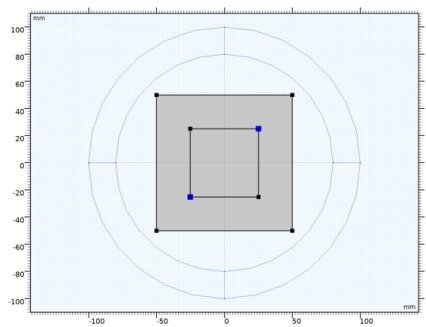
On the object sq1, select Points 1 and 3 only.
It might be easier to select the correct points by using the Selection List window. To open this window, in the Home toolbar click Windows and choose Selection List. (If you are running the cross-platform desktop, you find Windows in the main menu.)
3
In the Settings window for Chamfer, locate the Distance section.
4
In the Distance from vertex text field, type ch_d.
Extrude 1 (ext1)
1
In the Model Builder window, right-click Geometry 1 and choose Extrude.
2
In the Settings window for Extrude, locate the Distances section.
3
Cylinder 1 (cyl1)
1
In the Geometry toolbar, click  Cylinder.
2
In the Settings window for Cylinder, locate the Size and Shape section.
3
In the Radius text field, type 0.5.
4
In the Height text field, type thickness+2.
5
Locate the Position section. In the y text field, type -probe_l.
6
In the z text field, type -2.
Cylinder 2 (cyl2)
1
In the Geometry toolbar, click  Cylinder.
2
In the Settings window for Cylinder, locate the Size and Shape section.
3
In the Radius text field, type 2.05.
4
In the Height text field, type 2.
5
Locate the Position section. In the y text field, type -probe_l.
6
In the z text field, type -2.
7
Click  Build All Objects.
The finished geometry should look like this.
Definitions
Perfectly Matched Layer 1 (pml1)
1
In the Definitions toolbar, click  Perfectly Matched Layer.
2
3
In the Settings window for Perfectly Matched Layer, locate the Geometry section.
4
From the Type list, choose Spherical.
Electromagnetic Waves, Frequency Domain (emw)
Perfect Electric Conductor 2
1
In the Model Builder window, under Component 1 (comp1) right-click Electromagnetic Waves, Frequency Domain (emw) and choose Perfect Electric Conductor.
2
In the Settings window for Perfect Electric Conductor, locate the Boundary Selection section.
3
Click  Paste Selection.
4
In the Paste Selection dialog box, Select all metal parts.
5
type 15, 20-21, 24-25, 28-32, 34, 42-47 in the Selection text field.
6
Lumped Port 1
1
In the Physics toolbar, click  Boundaries and choose Lumped Port.
2
3
In the Settings window for Lumped Port, locate the Lumped Port Properties section.
4
From the Type of lumped port list, choose Coaxial.
For the first port, wave excitation is on by default.
Far-Field Domain 1
In the Physics toolbar, click  Domains and choose Far-Field Domain.
Add Material
1
In the Home toolbar, click  Add Material to open the Add Material window.
2
Go to the Add Material window.
3
4
Click Add to Component in the window toolbar.
5
In the Home toolbar, click  Add Material to close the Add Material window.
Materials
Material 2 (mat2)
1
In the Model Builder window, under Component 1 (comp1) right-click Materials and choose Blank Material.
2
3
In the Settings window for Material, locate the Material Contents section.
4
Material 3 (mat3)
1
Right-click Materials and choose Blank Material.
2
3
In the Settings window for Material, locate the Material Contents section.
4
Mesh 1
In the Model Builder window, under Component 1 (comp1) right-click Mesh 1 and choose Build All.
Definitions
Hide for Physics 1
1
In the Model Builder window, right-click View 1 and choose Hide for Physics.
2
In the Settings window for Hide for Physics, locate the Geometric Entity Selection section.
3
From the Geometric entity level list, choose Boundary.
4
Mesh 1
Study 1
In the Home toolbar, click  Compute.
Results
Multislice
1
In the Model Builder window, expand the Electric Field (emw) node, then click Multislice.
2
In the Settings window for Multislice, locate the Multiplane Data section.
3
Find the X-planes subsection. In the Planes text field, type 0.
4
Find the Y-planes subsection. In the Planes text field, type 0.
5
Find the Z-planes subsection. From the Entry method list, choose Coordinates.
6
In the Coordinates text field, type thickness/4.
7
In the Electric Field (emw) toolbar, click  Plot.
8
Click the  Zoom In button in the Graphics toolbar.
Compare the resulting plot with Figure 2.
Radiation Pattern 1
1
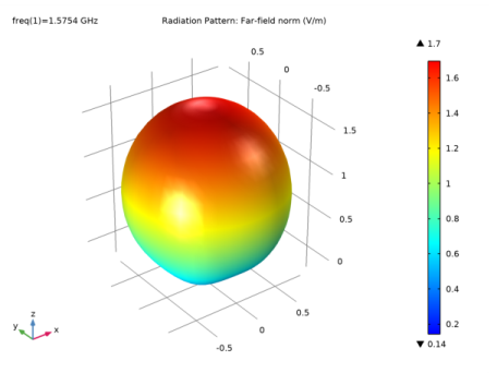
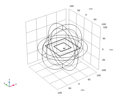
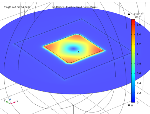
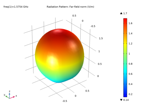
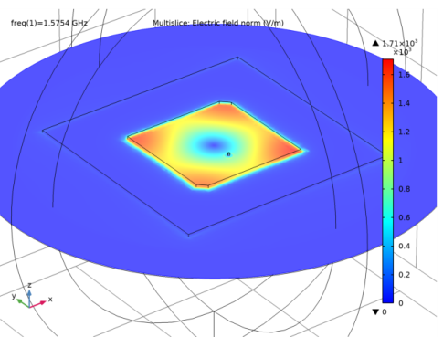
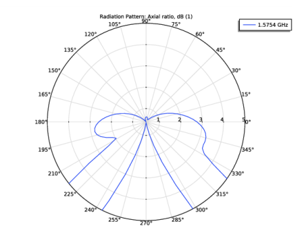
In the Model Builder window, expand the Results>2D Far Field (emw) node, then click Radiation Pattern 1.
2
In the Settings window for Radiation Pattern, locate the Expression section.
3
In the Expression text field, type emw.axialRatiodB.
4
Locate the Evaluation section. Find the Angles subsection. In the Number of angles text field, type 100.
5
Find the Reference direction subsection. In the x text field, type 0.
6
In the y text field, type 1.
7
Find the Normal vector subsection. In the x text field, type 1.
8
In the z text field, type 0.
9
In the 2D Far Field (emw) toolbar, click  Plot.
2D Far Field (emw)
1
In the Model Builder window, click 2D Far Field (emw).
2
In the Settings window for Polar Plot Group, locate the Axis section.
3
Select the Manual axis limits check box.
4
In the r maximum text field, type 5.
5
In the 2D Far Field (emw) toolbar, click  Plot.
3D Far Field (emw)
The axial ratio in a polar format is shown in Figure 3.
Radiation Pattern 1
See the 3D radiation pattern plotted in Figure 4.
Inspect the input matching (S11) at the simulated frequency.
6
In the Model Builder window, expand the Results>3D Far Field (emw) node.