|
|
|
|
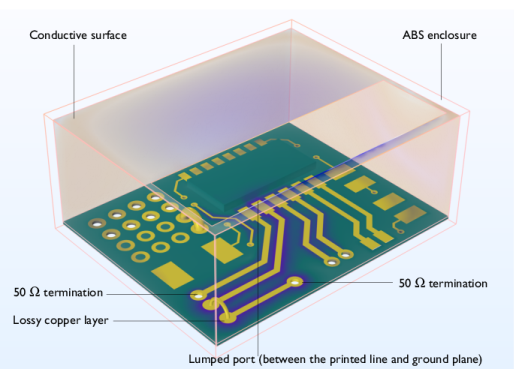
50 Ω via termination
|
|||
|
50 Ω via termination
|
|||

|
1
|
|
2
|
|
3
|
Click Add.
|
|
4
|
Click
|
|
5
|
|
6
|
Click
|
|
1
|
|
2
|
|
3
|
|
1
|
|
2
|
|
3
|
Click Browse.
|
|
4
|
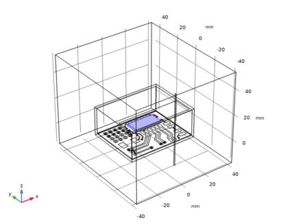
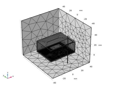
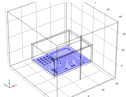
Browse to the model’s Application Libraries folder and double-click the file circuit_emiemc.mphbin.
|
|
5
|
Locate the Selections of Resulting Entities section. Select the Resulting objects selection check box.
|
|
6
|
|
1
|
|
2
|
|
3
|
|
4
|
|
5
|
|
6
|
|
7
|
|
8
|
|
1
|
|
2
|
|
3
|
|
4
|
|
5
|
|
6
|
|
7
|
|
8
|
|
9
|
|
1
|
|
2
|
|
3
|
|
4
|
|
5
|
|
6
|
|
7
|
|
8
|
|
1
|
|
2
|
|
3
|
|
4
|
|
1
|
|
2
|
|
3
|
|
4
|
|
5
|
|
6
|
|
7
|
|
1
|
|
2
|
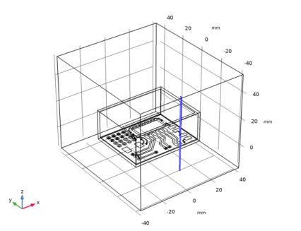
Select the object blk2 only.
|
|
3
|
|
4
|
|
5
|
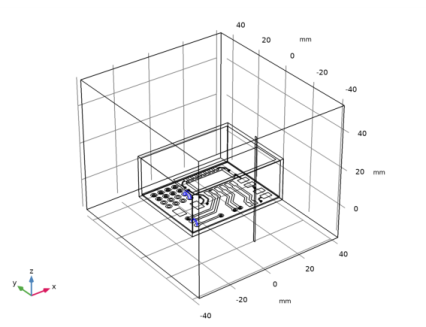
Select the object blk1 only.
|
|
6
|
|
1
|
|
2
|
|
3
|
|
4
|
|
5
|
|
6
|
|
7
|
|
8
|
|
1
|
|
2
|
|
3
|
|
1
|
|
2
|
|
3
|
|
4
|
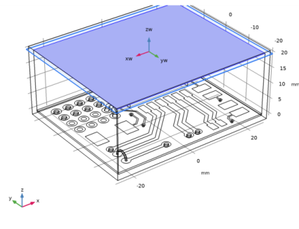
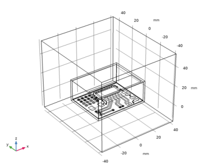
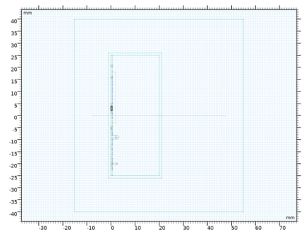
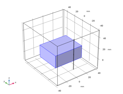
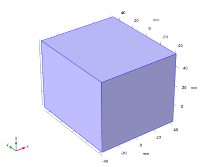
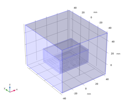
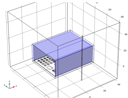
In the Height text field, type 55[mm]. The size is approximated for the antenna operating at the Wi-Fi frequency range
|
|
5
|
|
6
|
|
7
|
|
8
|
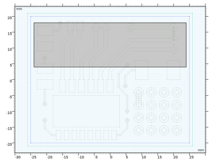
Click to expand the Layers section. In the table, enter the following settings:
|
|
9
|
|
1
|
|
2
|
|
3
|
|
4
|
|
1
|
|
2
|
|
3
|
|
4
|
|
5
|
|
6
|
|
7
|
|
8
|
|
1
|
|
2
|
|
3
|
|
4
|
|
1
|
|
2
|
|
3
|
|
4
|
|
1
|
|
2
|
|
3
|
|
4
|
|
1
|
|
2
|
|
3
|
In the tree, select Built-in>Air.
|
|
4
|
|
5
|
|
6
|
|
1
|
|
2
|
In the tree, select Built-in>Copper.
|
|
3
|
|
4
|
|
1
|
|
2
|
Locate the Geometric Entity Selection section. From the Geometric entity level list, choose Boundary.
|
|
3
|
|
1
|
|
2
|
|
4
|
|
1
|
|
2
|
|
4
|
|
1
|
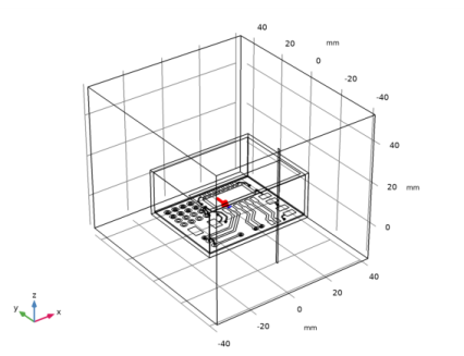
In the Model Builder window, under Component 1 (comp1) right-click Electromagnetic Waves, Frequency Domain (emw) and choose Lumped Port.
|
|
1
|
|
3
|
|
4
|
|
1
|
|
1
|
|
2
|
|
3
|
|
4
|
|
1
|
|
2
|
|
3
|
|
1
|
|
2
|
|
3
|
|
1
|
|
1
|
|
3
|
|
4
|
|
1
|
|
3
|
|
4
|
|
1
|
|
1
|
|
2
|
|
3
|
|
1
|
|
2
|
|
3
|
|
1
|
|
2
|
|
1
|
|
2
|
|
3
|
|
4
|
|
6
|
|
1
|
|
2
|
|
1
|
|
2
|
|
3
|
Click
|
|
4
|
|
5
|
|
6
|
|
7
|
Click Replace.
|
|
8
|
|
9
|
|
10
|
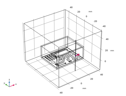
In the Physics and variables selection tree, select Component 1 (comp1)>Electromagnetic Waves, Frequency Domain (emw)>Lumped Port 2.
|
|
11
|
Click
|
|
12
|
In the Physics and variables selection tree, select Component 1 (comp1)>Electromagnetic Waves, Frequency Domain (emw)>Perfect Electric Conductor 2.
|
|
13
|
Click
|
|
14
|
|
1
|
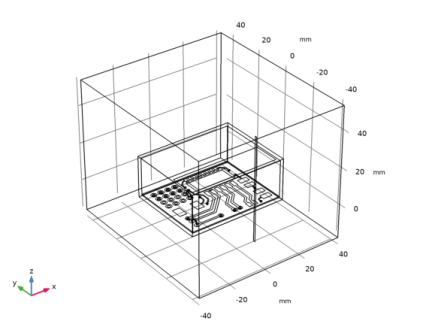
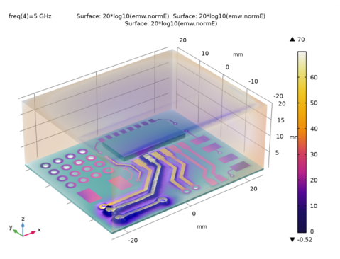
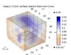
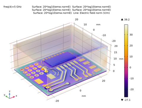
In the Model Builder window, expand the Results>Electric Field (emw) node, then click Electric Field (emw).
|
|
2
|
|
3
|
|
1
|
|
2
|
In the Settings window for 3D Plot Group, type Electric Field (emw) - Circuit Board in the Label text field.
|
|
1
|
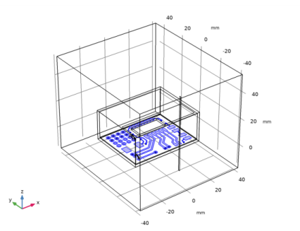
In the Model Builder window, right-click Surface 1 and choose Selection. The Selection subfeature let you plot the results only on the desired boundaries.
|
|
2
|
|
3
|
|
4
|
|
1
|
|
2
|
|
3
|
|
4
|
|
1
|
|
2
|
|
3
|
|
4
|
|
5
|
|
6
|
|
1
|
|
2
|
|
3
|
|
1
|
|
2
|
|
3
|
|
4
|
|
1
|
|
2
|
|
3
|
|
1
|
|
2
|
|
3
|
|
4
|
|
1
|
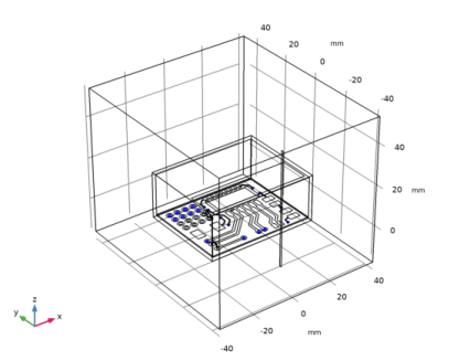
Right-click Surface 3 and choose Transparency. Using the Transparency subfeature, the plot can be partially transparent.
|
|
2
|
|
3
|
|
1
|
|
2
|
|
3
|
|
4
|
|
1
|
|
2
|
|
3
|
|
1
|
|
2
|
|
3
|
|
4
|
|
1
|
|
2
|
|
3
|
|
4
|
|
1
|
|
2
|
|
3
|
|
4
|
|
1
|
|
2
|
|
3
|
|
4
|
|
5
|
|
6
|
|
1
|
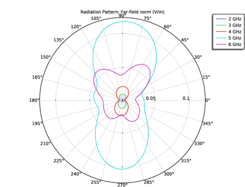
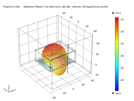
In the Model Builder window, expand the Results>3D Far Field (emw) node, then click Radiation Pattern 1.
|
|
2
|
|
3
|
|
1
|
|
1
|
|
2
|
|
3
|
|
4
|
|
1
|
|
2
|
|
3
|
|
4
|
|
5
|
|
6
|
|
1
|
|
3
|
|
1
|
|
2
|
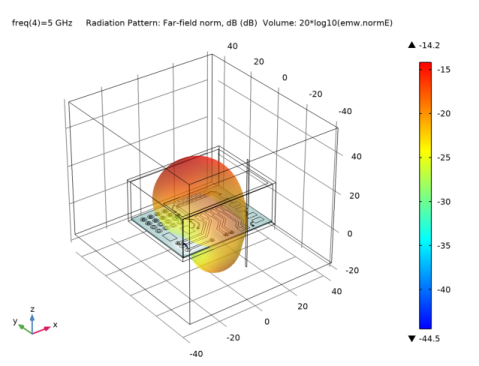
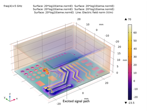
In the Settings window for 3D Plot Group, type Radiated Emission - Near Field in the Label text field.
|
|
3
|
|
1
|
|
2
|
|
1
|
|
1
|
|
2
|
|
3
|
|
1
|
|
2
|
|
3
|
|
4
|
|
5
|
|
6
|
|
7
|
|
8
|
|
1
|
|
2
|
|
3
|
|
4
|
|
5
|
|
1
|
|
2
|
|
4
|
|
1
|
|
2
|
|
3
|
|
4
|
|
5
|
|
1
|
|
2
|
|
4
|
|
1
|
|
2
|
|
3
|
|
4
|
|
5
|
|
1
|
|
2
|
|
3
|
Locate the Study Settings section. Clear the Generate default plots check box. The default plots will not be generated. Instead, some of the plots from the first study will be duplicated after computation.
|
|
1
|
|
2
|
|
3
|
|
4
|
Locate the Physics and Variables Selection section. Select the Modify model configuration for study step check box.
|
|
5
|
In the Physics and variables selection tree, select Component 1 (comp1)>Electromagnetic Waves, Frequency Domain (emw)>Lumped Port 1.
|
|
6
|
Click
|
|
7
|
In the Physics and variables selection tree, select Component 1 (comp1)>Electromagnetic Waves, Frequency Domain (emw)>Far-Field Domain 1.
|
|
8
|
Click
|
|
9
|
|
1
|
|
2
|
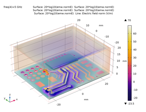
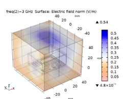
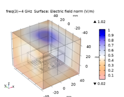
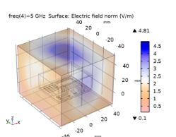
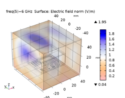
In the Settings window for 3D Plot Group, type Electric Field (emw) - Circuit Board, Immunity in the Label text field.
|
|
3
|
|
4
|
|
5
|
|
6
|
|
1
|
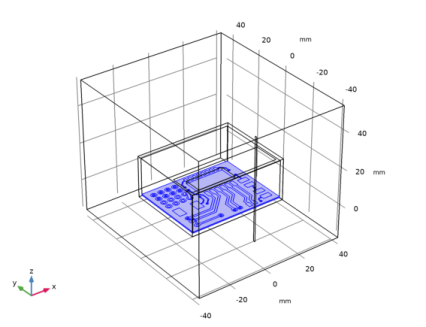
In the Model Builder window, expand the Results>Electric Field (emw) - Circuit Board, Immunity>Surface 1 node, then click Deformation 1.
|
|
2
|
|
3
|
|
1
|
In the Model Builder window, expand the Results>Electric Field (emw) - Circuit Board, Immunity>Surface 2 node, then click Deformation 1.
|
|
2
|
|
3
|
|
4
|
In the Electric Field (emw) - Circuit Board, Immunity toolbar, click
 |
|
1
|
|
2
|
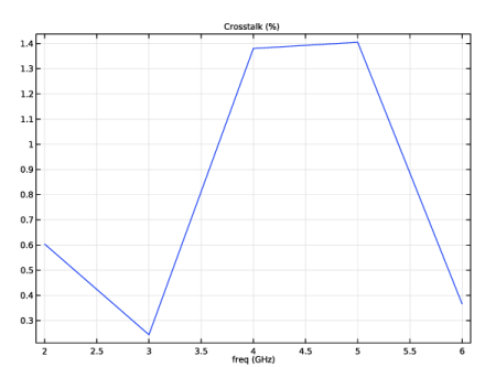
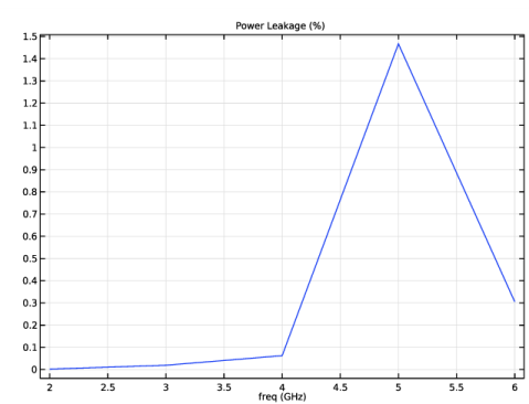
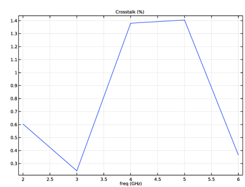
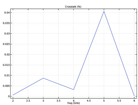
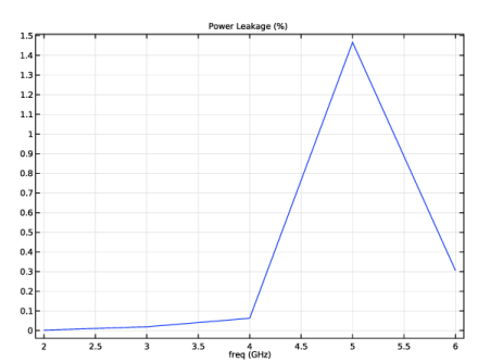
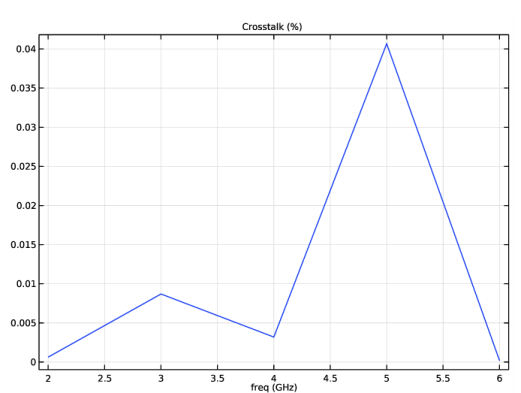
In the Settings window for 1D Plot Group, type Noise Coupling to Signal Line in the Label text field.
|
|
3
|
|
1
|
|
2
|
|
4
|
|
1
|
|
2
|