PDF

Branch-Line Coupler
Introduction
A branch line coupler, also known as a quadrature (90°) hybrid, is a four-port network device with one input port, two output ports, with a 90° phase difference between them, and one isolated port. Due to its symmetry, any port can be used as the input port.
Figure 1: The geometry of a branch line coupler is symmetric.
Model Definition
The form of the branch line coupler is shown schematically in Figure 1. The layout design is based upon Ref. 1, and is tuned to operate at 3 GHz. The design is realized as microstrip lines patterned onto a 0.060 inch dielectric substrate. The microstrip lines are modeled as perfect electric conductor (PEC) surfaces, and another PEC surface on the bottom of the dielectric substrate acts as a ground plane. The entire modeling domain is bounded by PEC boundaries that represent the device packaging. The four ports are modeled as small rectangular faces that bridge the gap between the PEC face that represents the ground plane, and the PEC faces that represent the microstrip line at each port.
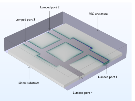
Figure 2: The model of the branch line coupler. Some exterior faces are removed for visualization.
The model is shown in Figure 2. A small air domain bounded by a PEC surface around the device is also modeled. The model is meshed using a tetrahedral mesh. A good rule of thumb is to use approximately five elements per wavelength in each material. The physics-controlled mesh is used to generate the mesh automatically.
After the first study, the model is modified to utilized the SMA connector in the part library. The SMA connector with two holes at the flange is added at each end of the microstrip line and the type of lumped port is changed from uniform to coaxial.
Results and Discussion
The computed S-parameters are plotted in Figure 3. At a frequency of 3 GHz, the signal is evenly split between the two output ports with a very small amount of losses. The input signal is barely coupled to the isolation port where S41 is less than 30 dB at 3 GHz. The evaluated phase shift between the two output ports is 89.9°.
Figure 3: The frequency response of the branch line coupler shows good input matching (S11) and isolation (S41) around 3 GHz. The coupled signal at the two output ports (S21 and S31) is about -3 dB at 3 GHz.
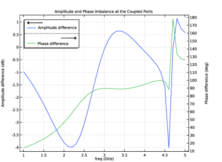
Figure 4: The amplitude and phase imbalance on the two output ports. The phase difference at 3 GHz is approximately 90 degrees.
Because the metallic housing works as a rectangular cavity, there is a resonance observed around 4.6 GHz. The resonant frequency of an air-filled hollow rectangular cavity is
where a and b are the dimensions of the sidewall of the cavity and d is the length of the cavity. The dominant resonant frequency at TE101 mode is close to 5 GHz. Because the cavity is partially filled by the dielectric substrate, the resonance is expected lower than the that of the air-filled cavity. This resonance can easily be removed by adding a metallic post in the middle of the cavity connecting the bottom ground plane to the top ceiling if necessary.
The results after adding the SMA connectors are similar to those without the connectors and they are presented in the step by step instructions.
Reference
1. D.M. Pozar, Microwave Engineering, John Wiley & Sons, 1998.
Application Library path: RF_Module/Couplers_and_Power_Dividers/branch_line_coupler
Modeling Instructions
From the File menu, choose New.
New
In the New window, click  Model Wizard.
Model Wizard
1
In the Model Wizard window, click  3D.
2
In the Select Physics tree, select Radio Frequency>Electromagnetic Waves, Frequency Domain (emw).
3
Click Add.
4
Click  Study.
5
In the Select Study tree, select General Studies>Frequency Domain.
6
Study 1
Step 1: Frequency Domain
1
In the Model Builder window, under Study 1 click Step 1: Frequency Domain.
2
In the Settings window for Frequency Domain, locate the Study Settings section.
3
In the Frequencies text field, type range(1[GHz],100[MHz],5[GHz]).
Global Definitions
Parameters 1
1
In the Model Builder window, under Global Definitions click Parameters 1.
2
In the Settings window for Parameters, locate the Parameters section.
3
Here, mil refers to the unit milliinch.
Geometry 1
1
In the Model Builder window, under Component 1 (comp1) click Geometry 1.
2
In the Settings window for Geometry, locate the Units section.
3
From the Length unit list, choose mm.
Work Plane 1 (wp1)
1
In the Geometry toolbar, click  Work Plane, to add an xy-plane for the coupler layout’.
2
In the Settings window for Work Plane, click  Show Work Plane.
Work Plane 1 (wp1)>Plane Geometry
In the Model Builder window, click Plane Geometry.
Work Plane 1 (wp1)>Rectangle 1 (r1)
1
In the Work Plane toolbar, click  Rectangle.
2
In the Settings window for Rectangle, locate the Size and Shape section.
3
In the Width text field, type 2*w_line1+l_line3.
4
In the Height text field, type l_s.
5
Locate the Position section. From the Base list, choose Center.
6
Click  Build Selected.
Work Plane 1 (wp1)>Rectangle 2 (r2)
1
In the Work Plane toolbar, click  Rectangle.
2
In the Settings window for Rectangle, locate the Size and Shape section.
3
In the Width text field, type w_line2*2+l_line3.
4
In the Height text field, type l_line2.
5
Locate the Position section. From the Base list, choose Center.
6
In the Work Plane toolbar, click  Build All.
Work Plane 1 (wp1)>Rectangle 3 (r3)
1
In the Work Plane toolbar, click  Rectangle.
2
In the Settings window for Rectangle, locate the Size and Shape section.
3
In the Width text field, type l_line3.
4
In the Height text field, type l_line2.
5
Locate the Position section. In the xw text field, type -l_line3/2.
6
In the yw text field, type l_line2/2+w_line3.
7
Click  Build Selected.
8
Click the  Zoom Extents button in the Graphics toolbar.
Work Plane 1 (wp1)>Array 1 (arr1)
1
In the Work Plane toolbar, click  Transforms and choose Array.
2
3
In the Settings window for Array, locate the Size section.
4
From the Array type list, choose Linear.
5
In the Size text field, type 3.
6
Locate the Displacement section. In the yw text field, type -l_line2-w_line3.
7
In the Work Plane toolbar, click  Build All.
Work Plane 1 (wp1)>Difference 1 (dif1)
1
In the Work Plane toolbar, click  Booleans and Partitions and choose Difference.
2
Select the objects r1 and r2 only.
3
In the Settings window for Difference, locate the Difference section.
4
Find the Objects to subtract subsection. Select the  Activate Selection toggle button.
5
Select the objects arr1(1), arr1(2), and arr1(3) only, the three rectangles belonging to the array object (arr1).
6
Clear the Keep interior boundaries check box.
7
In the Work Plane toolbar, click  Build All.
Work Plane 1 (wp1)
Extrude the xy-plane with the thickness of the substrate. Additional rectangular boundaries at each end of the feed lines are created by this extrusion, too. Use these boundaries to assign lumped ports later.
Extrude 1 (ext1)
1
In the Model Builder window, under Component 1 (comp1)>Geometry 1 right-click Work Plane 1 (wp1) and choose Extrude.
2
In the Settings window for Extrude, locate the Distances section.
3
4
Click  Build All Objects.
5
Click the  Zoom Extents button in the Graphics toolbar.
Choose wireframe rendering to get a better view of the interior parts.
6
Click the  Wireframe Rendering button in the Graphics toolbar.
Create a block for the substrate.
Block 1 (blk1)
1
In the Geometry toolbar, click  Block.
2
In the Settings window for Block, locate the Size and Shape section.
3
In the Width text field, type l_s.
4
In the Depth text field, type l_s.
5
In the Height text field, type thickness.
6
Locate the Position section. From the Base list, choose Center.
7
In the z text field, type thickness/2.
8
Click  Build All Objects.
Substrate
1
In the Geometry toolbar, click  Booleans and Partitions and choose Union.
2
In the Settings window for Union, type Substrate in the Label text field.
3
Locate the Union section. Clear the Keep interior boundaries check box.
4
Click in the Graphics window and then press Ctrl+A to select both objects.
5
Locate the Selections of Resulting Entities section. Select the Resulting objects selection check box.
6
Click  Build All Objects.
Package
1
In the Geometry toolbar, click  Block.
2
In the Settings window for Block, type Package in the Label text field.
3
Locate the Size and Shape section. In the Width text field, type l_s.
4
In the Depth text field, type l_s+l_s/8.
5
In the Height text field, type thickness*5.
6
Locate the Position section. From the Base list, choose Center.
7
In the z text field, type thickness*5/2.
8
Click  Build All Objects.
The completed geometry describes the microstrip line device on a substrate enclosed by a metal housing.
Definitions
View 1
Hide three boundaries to get a better view of the interior parts when reviewing the mesh.
Hide for Physics 1
1
In the Model Builder window, expand the Component 1 (comp1)>Definitions node.
2
Right-click View 1 and choose Hide for Physics.
3
In the Settings window for Hide for Physics, locate the Geometric Entity Selection section.
4
From the Geometric entity level list, choose Boundary.
5
It might be easier to select the boundaries by using the Selection List window. To open this window, in the Home toolbar click Windows and choose Selection List. (If you are running the cross-platform desktop, you find Windows in the main menu.)
Electromagnetic Waves, Frequency Domain (emw)
Now set up the physics. The default boundary condition is perfect electric conductor, which is applied to all exterior boundaries. Apply this condition also to the interior boundaries of the microstrip lines.
Perfect Electric Conductor 2
1
In the Model Builder window, under Component 1 (comp1) right-click Electromagnetic Waves, Frequency Domain (emw) and choose Perfect Electric Conductor.
2
Lumped Port 1
1
In the Physics toolbar, click  Boundaries and choose Lumped Port.
2
For the first port, wave excitation is on by default.
Lumped Port 2
1
In the Physics toolbar, click  Boundaries and choose Lumped Port.
2
Lumped Port 3
1
In the Physics toolbar, click  Boundaries and choose Lumped Port.
2
Lumped Port 4
1
In the Physics toolbar, click  Boundaries and choose Lumped Port.
2
Lumped ports are assigned at each end of the microstrip lines. Wave excitation is on only at the first port.
Materials
Assign material properties to the model. First, apply air to all domains.
Add Material
1
In the Home toolbar, click  Add Material to open the Add Material window.
2
Go to the Add Material window.
3
4
Click Add to Component in the window toolbar.
5
In the Home toolbar, click  Add Material to close the Add Material window.
Materials
Create a dielectric material of er = 3.38 overriding air in the substrate.
Substrate
1
In the Model Builder window, under Component 1 (comp1) right-click Materials and choose Blank Material.
2
In the Settings window for Material, type Substrate in the Label text field.
3
Locate the Geometric Entity Selection section. From the Selection list, choose Substrate.
4
Locate the Material Contents section. In the table, enter the following settings:
Mesh 1
1
In the Model Builder window, under Component 1 (comp1) right-click Mesh 1 and choose Build All.
Three exterior boundaries are hidden in this view.
Study 1
In the Home toolbar, click  Compute.
Results
Electric Field (emw)
Begin the results analysis and visualization by modifying the first default plot to show the E-field norm in the middle of the substrate at 3 GHz.
1
In the Settings window for 3D Plot Group, locate the Data section.
2
From the Parameter value (freq (GHz)) list, choose 3.
Multislice
1
In the Model Builder window, expand the Electric Field (emw) node, then click Multislice.
2
In the Settings window for Multislice, locate the Multiplane Data section.
3
Find the X-planes subsection. In the Planes text field, type 0.
4
Find the Y-planes subsection. In the Planes text field, type 0.
5
Find the Z-planes subsection. From the Entry method list, choose Coordinates.
6
In the Coordinates text field, type thickness/2.
7
In the Electric Field (emw) toolbar, click  Plot.
The input power is evenly split between the two output ports.
S-parameter (emw)
1
In the Model Builder window, click S-parameter (emw).
2
In the Settings window for 1D Plot Group, click to expand the Title section.
3
Locate the Legend section. From the Position list, choose Lower right.
Compare the resulting plot with that shown in Figure 3.
Smith Plot (emw)
Plot the amplitude and phase imbalance on two output ports (Figure 4).
Imbalance
1
In the Home toolbar, click  Add Plot Group and choose 1D Plot Group.
2
In the Settings window for 1D Plot Group, type Imbalance in the Label text field.
3
Locate the Title section. From the Title type list, choose Manual.
4
In the Title text area, type Amplitude and Phase Imbalance at the Coupled Ports.
5
Locate the Legend section. From the Position list, choose Upper left.
Global 1
1
Right-click Imbalance and choose Global.
2
In the Settings window for Global, locate the y-Axis Data section.
3
Global 2
1
In the Model Builder window, right-click Imbalance and choose Global.
2
In the Settings window for Global, locate the y-Axis Data section.
3
The unit is degree.
Imbalance
1
In the Model Builder window, click Imbalance.
2
In the Settings window for 1D Plot Group, locate the Plot Settings section.
3
Select the Two y-axes check box.
4
In the table, select the Plot on secondary y-axis check box for Global 2.
5
In the Imbalance toolbar, click  Plot.
The phase difference between two output ports is approximately 90 degrees at 3 GHz.
Evaluate the phase difference between two output ports at 3 GHz.
Global Evaluation 1
1
In the Results toolbar, click  Global Evaluation.
2
In the Settings window for Global Evaluation, locate the Data section.
3
From the Parameter selection (freq) list, choose From list.
4
In the Parameter values (freq (GHz)) list, select 3.
5
Locate the Expressions section. In the table, enter the following settings:
6
Click  Evaluate.
When the designed circuit is measured with a network analyzer, the circuit is connected to cables through connectors. Those connectors are not part of the network analyzer calibration process, and they may change the frequency response due to an additional reactive loading. By adding connectors, the simulation becomes closer to the real world device. The RF part library helps to quickly add SMA connectors to the coupler without handling multiple geometry operations.
Global Definitions
Parameters 1
1
In the Model Builder window, under Global Definitions click Parameters 1.
2
In the Settings window for Parameters, locate the Parameters section.
3
Geometry 1
Package (blk2)
1
In the Model Builder window, under Component 1 (comp1)>Geometry 1 click Package (blk2).
2
In the Settings window for Block, locate the Position section.
3
In the z text field, type thickness+0.635.
4
Locate the Size and Shape section. In the Depth text field, type l_s.
5
In the Height text field, type 20.
6
Click  Build Selected.
Part Libraries
1
In the Home toolbar, click  Windows and choose Part Libraries.
2
In the Model Builder window, click Geometry 1.
3
In the Part Libraries window, select RF Module>Connectors>connector_sma_flange2 in the tree.
4
Click  Add to Geometry.
Geometry 1
SMA Connector, Flange with Two Holes 1 (pi1)
1
In the Model Builder window, under Component 1 (comp1)>Geometry 1 click SMA Connector, Flange with Two Holes 1 (pi1).
2
In the Settings window for Part Instance, locate the Input Parameters section.
3
4
Locate the Position and Orientation of Output section. Find the Displacement subsection. In the xw text field, type -8.4.
5
In the yw text field, type -l_s/2.
6
In the zw text field, type thickness+0.635.
7
Find the Rotation subsection. In the Rotation angle text field, type 90.
8
Click to expand the Domain Selections section. In the table, enter the following settings:
9
Click to expand the Boundary Selections section. In the table, enter the following settings:
10
Click  Build All Objects.
Copy 1 (copy1)
1
In the Geometry toolbar, click  Transforms and choose Copy.
2
3
In the Settings window for Copy, locate the Displacement section.
4
In the x text field, type 16.8.
Rotate 1 (rot1)
1
In the Geometry toolbar, click  Transforms and choose Rotate.
2
Select the objects copy1 and pi1 only.
3
In the Settings window for Rotate, locate the Rotation section.
4
In the Angle text field, type 0 180.
5
Click  Build All Objects.
The duplicated trace on the bottom ground plane can be removed as necessary. In this model, it is optional.
Form Composite Faces 1 (cmf1)
1
In the Geometry toolbar, click  Virtual Operations and choose Form Composite Faces.
2
On the object fin, select Boundaries 6, 44, 153, 156, 158, and 319 only.
3
In the Geometry toolbar, click  Build All.
Electromagnetic Waves, Frequency Domain (emw)
Perfect Electric Conductor 2
1
In the Model Builder window, under Component 1 (comp1)>Electromagnetic Waves, Frequency Domain (emw) click Perfect Electric Conductor 2.
2
Lumped Port 1
1
In the Model Builder window, click Lumped Port 1.
2
In the Settings window for Lumped Port, locate the Boundary Selection section.
3
Click  Clear Selection.
4
5
Locate the Lumped Port Properties section. From the Type of lumped port list, choose Coaxial.
Lumped Port 2
1
In the Model Builder window, click Lumped Port 2.
2
In the Settings window for Lumped Port, locate the Boundary Selection section.
3
Click  Clear Selection.
4
5
Locate the Lumped Port Properties section. From the Type of lumped port list, choose Coaxial.
Lumped Port 3
1
In the Model Builder window, click Lumped Port 3.
2
In the Settings window for Lumped Port, locate the Boundary Selection section.
3
Click  Clear Selection.
4
5
Locate the Lumped Port Properties section. From the Type of lumped port list, choose Coaxial.
Lumped Port 4
1
In the Model Builder window, click Lumped Port 4.
2
In the Settings window for Lumped Port, locate the Boundary Selection section.
3
Click  Clear Selection.
4
5
Locate the Lumped Port Properties section. From the Type of lumped port list, choose Coaxial.
Perfect Electric Conductor 3
1
In the Physics toolbar, click  Boundaries and choose Perfect Electric Conductor.
2
In the Settings window for Perfect Electric Conductor, locate the Boundary Selection section.
3
From the Selection list, choose Conductive surface (SMA Connector, Flange with Two Holes 1).
Materials
Material 3 (mat3)
1
In the Model Builder window, under Component 1 (comp1) right-click Materials and choose Blank Material.
2
In the Settings window for Material, locate the Geometric Entity Selection section.
3
From the Selection list, choose Dielectric (SMA Connector, Flange with Two Holes 1).
4
Locate the Material Contents section. In the table, enter the following settings:
Mesh 1
1
In the Model Builder window, under Component 1 (comp1) right-click Mesh 1 and choose Build All.
2
In the Home toolbar, click  Compute.
Results
Multislice
1
In the Model Builder window, under Results>Electric Field (emw) click Multislice.
2
In the Settings window for Multislice, locate the Coloring and Style section.
3
From the Color table list, choose HeatCameraLight.
4
Select the Reverse color table check box.
Surface 1
1
In the Model Builder window, right-click Electric Field (emw) and choose Surface.
2
In the Settings window for Surface, locate the Coloring and Style section.
3
From the Color table list, choose AuroraAustralis.
4
Clear the Color legend check box.
Selection 1
1
Right-click Surface 1 and choose Selection.
2
In the Settings window for Selection, locate the Selection section.
3
From the Selection list, choose Conductive surface (SMA Connector, Flange with Two Holes 1).
4
In the Electric Field (emw) toolbar, click  Plot.
S-parameter (emw)
Smith Plot (emw)
Imbalance