
|
|
|


|
|
|||
|
1
|
|
2
|
|
3
|
Click Add.
|
|
4
|
Click
|
|
5
|
|
6
|
Click
|
|
1
|
|
2
|
In the Show More Options dialog box, in the tree, select the check box for the node Physics>Advanced Physics Options.
|
|
3
|
Click OK.
|
|
1
|
|
2
|
|
1
|
|
2
|
|
3
|
|
4
|
|
5
|
|
1
|
|
2
|
|
3
|
|
4
|
|
5
|
|
1
|
|
2
|
|
3
|
|
4
|
|
5
|
|
6
|
|
1
|
|
2
|
|
3
|
|
4
|
|
5
|
|
1
|
|
2
|
|
3
|
|
4
|
|
5
|
|
6
|
|
1
|
|
2
|
|
3
|
|
4
|
|
5
|
|
6
|
|
1
|
|
2
|
|
3
|
|
4
|
|
5
|
|
6
|
|
1
|
|
2
|
|
3
|
|
4
|
|
5
|
|
6
|
|
1
|
|
2
|
|
3
|
|
4
|
|
5
|
|
1
|
|
2
|
|
3
|
|
4
|
|
5
|
|
1
|
|
2
|
|
3
|
|
4
|
|
5
|
|
6
|
|
7
|
|
8
|
|
9
|
|
1
|
|
2
|
|
1
|
|
2
|
|
3
|
|
4
|
|
5
|
|
6
|
|
7
|
Click
|
|
1
|
|
2
|
|
3
|
|
1
|
|
2
|
|
3
|
|
5
|
|
6
|
|
7
|
Click OK.
|
|
1
|
|
2
|
|
3
|
|
1
|
In the Model Builder window, under Component 1 (comp1) right-click Materials and choose Blank Material.
|
|
3
|
|
1
|
|
3
|
|
1
|
|
3
|
|
1
|
|
3
|
|
4
|
|
1
|
In the Model Builder window, under Component 1 (comp1) right-click Magnetic Fields (mf) and choose the domain setting Coil.
|
|
3
|
|
4
|
|
5
|
|
6
|
|
7
|
|
1
|
|
1
|
|
2
|
|
3
|
|
4
|
Click the Custom button.
|
|
5
|
|
6
|
|
1
|
|
1
|
|
2
|
|
3
|
|
4
|
Click the Custom button.
|
|
5
|
|
6
|
|
1
|
|
2
|
|
3
|
|
1
|
|
2
|
|
3
|
|
1
|
|
2
|
|
3
|
|
1
|
|
2
|
|
3
|
|
4
|
Click the Custom button.
|
|
5
|
|
6
|
|
1
|
|
2
|
|
1
|
|
2
|
|
3
|
|
4
|
|
5
|
|
6
|
|
7
|
|
8
|
|
9
|
|
11
|
|
12
|
|
13
|
|
14
|
|
1
|
|
1
|
|
2
|
|
3
|
|
1
|
|
2
|
In the Settings window for 2D Plot Group, type Stationary Magnetic Flux Density in the Label text field.
|
|
1
|
|
2
|
|
3
|
|
4
|
|
5
|
|
6
|
|
7
|
|
8
|
|
1
|
|
2
|
|
3
|
|
4
|
|
5
|
|
6
|
|
1
|
|
2
|
In the Settings window for Contour, click Replace Expression in the upper-right corner of the Expression section. From the menu, choose Component 1 (comp1)>Magnetic Fields>Magnetic>mf.normB - Magnetic flux density norm - T.
|
|
3
|
|
4
|
Click
|
|
5
|
|
6
|
|
7
|
|
8
|
|
9
|
Click Replace.
|
|
10
|
|
1
|
|
2
|
|
3
|
Locate the Data section. From the Dataset list, choose Study 1/Adaptive Mesh Refinement Solutions 1 (sol2).
|
|
1
|
|
2
|
|
3
|
|
4
|
|
5
|
|
6
|
Click Define custom colors.
|
|
8
|
Click Add to custom colors.
|
|
9
|
|
10
|
|
1
|
|
2
|
|
3
|
|
4
|
Find the Physics interfaces in study subsection. In the table, clear the Solve check box for Study 1.
|
|
5
|
|
6
|
|
1
|
In the Model Builder window, under Component 1 (comp1) click Electromagnetic Waves, Frequency Domain (emw).
|
|
2
|
In the Settings window for Electromagnetic Waves, Frequency Domain, locate the Domain Selection section.
|
|
3
|
|
1
|
|
2
|
|
3
|
|
4
|
|
5
|
Locate the Plasma Properties section. Select the Compute tensor electron transport properties check box.
|
|
1
|
In the Model Builder window, under Component 1 (comp1)>Multiphysics click Plasma Conductivity Coupling 1 (pcc1).
|
|
2
|
In the Settings window for Plasma Conductivity Coupling, locate the Compute Tensor Plasma Conductivity section.
|
|
3
|
|
4
|
|
1
|
|
2
|
|
3
|
|
1
|
|
2
|
|
3
|
Click Browse.
|
|
5
|
Click Import.
|
|
1
|
|
2
|
|
3
|
|
4
|
|
1
|
|
2
|
|
3
|
|
4
|
|
1
|
|
2
|
|
3
|
|
4
|
|
1
|
|
2
|
|
3
|
|
4
|
|
1
|
|
2
|
|
3
|
|
4
|
|
5
|
Locate the Mobility and Diffusivity Expressions section. From the Specification list, choose Specify mobility, compute diffusivity.
|
|
6
|
|
7
|
|
8
|
Browse to the model’s Application Libraries folder and double-click the file ion_mobility_data.txt.
|
|
1
|
|
2
|
|
3
|
|
4
|
|
1
|
|
2
|
|
3
|
|
4
|
|
1
|
|
2
|
|
3
|
|
1
|
|
2
|
|
3
|
|
1
|
|
2
|
|
3
|
|
1
|
|
2
|
|
3
|
|
4
|
|
5
|
|
6
|
|
1
|
|
3
|
|
4
|
|
5
|
|
6
|
|
1
|
|
2
|
|
3
|
|
1
|
|
2
|
|
3
|
|
5
|
|
1
|
|
2
|
|
3
|
|
1
|
|
2
|
|
3
|
|
4
|
|
5
|
|
6
|
|
1
|
|
2
|
|
3
|
Find the Physics interfaces in study subsection. In the table, clear the Solve check box for Magnetic Fields (mf).
|
|
4
|
Find the Studies subsection. In the Select Study tree, select Preset Studies for Selected Multiphysics>Frequency-Transient.
|
|
5
|
|
6
|
|
1
|
|
2
|
|
3
|
|
4
|
Locate the Physics and Variables Selection section. In the table, clear the Solve for check box for Magnetic Fields (mf).
|
|
5
|
|
6
|
Click to expand the Values of Dependent Variables section. Find the Values of variables not solved for subsection. From the Settings list, choose User controlled.
|
|
7
|
|
8
|
|
9
|
|
10
|
|
1
|
|
2
|
|
3
|
|
4
|
|
5
|
|
1
|
|
2
|
|
3
|
|
1
|
|
2
|
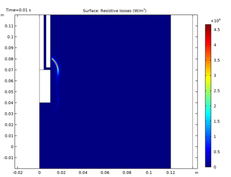
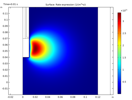
In the Settings window for Surface, click Replace Expression in the upper-right corner of the Expression section. From the menu, choose Component 1 (comp1)>Electromagnetic Waves, Frequency Domain>Heating and losses>emw.Qrh - Resistive losses - W/m³.
|
|
3
|
|
1
|
|
2
|
|
1
|
|
2
|
|
3
|
|
4
|
|
1
|
|
2
|
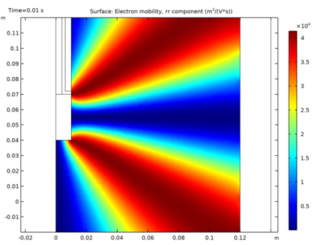
In the Settings window for 2D Plot Group, type Electron Mobility, rr Component in the Label text field.
|
|
1
|
|
2
|
In the Settings window for Surface, click Replace Expression in the upper-right corner of the Expression section. From the menu, choose Component 1 (comp1)>Plasma>Electron transport properties>Electron mobility - m²/(V·s)>plas.muerr - Electron mobility, rr component.
|
|
3
|
|
1
|
|
2
|
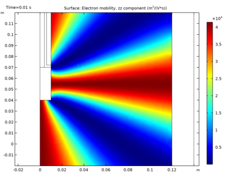
In the Settings window for 2D Plot Group, type Electron Mobility, zz Component in the Label text field.
|
|
1
|
|
2
|
In the Settings window for Surface, click Replace Expression in the upper-right corner of the Expression section. From the menu, choose Component 1 (comp1)>Plasma>Electron transport properties>Electron mobility - m²/(V·s)>plas.muezz - Electron mobility, zz component.
|
|
3
|
|
1
|
|
2
|
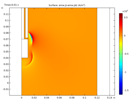
In the Settings window for 2D Plot Group, type Conduction Current Density, r-Component in the Label text field.
|
|
3
|
|
1
|
|
2
|
|
3
|
|
4
|
|
1
|
In the Model Builder window, right-click Conduction Current Density, r-Component and choose Duplicate.
|
|
2
|
In the Settings window for 2D Plot Group, type Conduction Current Density, z-Component in the Label text field.
|
|
1
|
In the Model Builder window, expand the Conduction Current Density, z-Component node, then click Surface 1.
|
|
2
|
|
3
|
|
4
|
|
1
|
In the Model Builder window, right-click Conduction Current Density, z-Component and choose Duplicate.
|
|
2
|
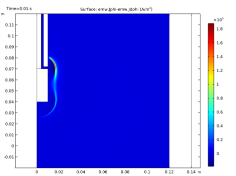
In the Settings window for 2D Plot Group, type Conduction Current Density, phi-Component in the Label text field.
|
|
1
|
In the Model Builder window, expand the Conduction Current Density, phi-Component node, then click Surface 1.
|
|
2
|
|
3
|
|
4
|
|
1
|
|
2
|
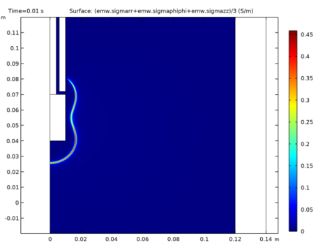
In the Settings window for 2D Plot Group, type Mean Plasma Electrical Conductivity in the Label text field.
|
|
1
|
In the Model Builder window, expand the Mean Plasma Electrical Conductivity node, then click Surface 1.
|
|
2
|
|
3
|
|
4
|