PDF

Surface Acoustic Wave Gas Sensor
Introduction
A surface acoustic wave (SAW) is an acoustic wave propagating along the surface of a solid material. Its amplitude decays rapidly, often exponentially, with the depth of the material. SAWs are featured in many kinds of electronic components, including filters, oscillators, and sensors. SAW devices typically use electrodes on a piezoelectric material to convert an electric signal to a SAW, and back again.
In this model, you investigate the resonance frequencies of a SAW gas sensor. The sensor consists of an interdigitated transducer (IDT) etched onto a piezoelectric LiNbO3 (lithium niobate) substrate and covered with a thin polyisobutylene (PIB) film. The mass of the PIB film increases as PIB selectively adsorbs CH2Cl2 (dichloromethane, DCM) from air. This causes a shift in resonance which slightly lowers the resonance frequency for the same SAW mode.
Model Definition
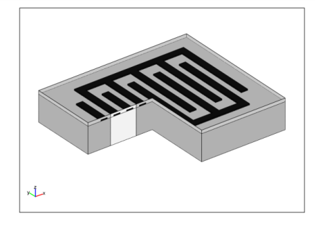
Figure 1 shows a conceptual view of the gas sensor in this model.
Figure 1: SAW gas sensor, showing the IDT electrodes (in black), the thin PIB film (light gray), and the LiNbO3 substrate (dark gray). For the sake of clarity, the dimensions are not to scale and the IDT has fewer electrodes than in common devices. A slice of the geometry is removed to reveal the modeled unit cell (in white).
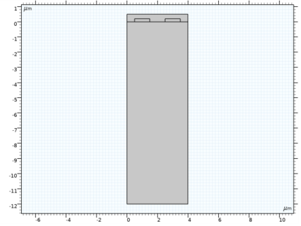
IDTs used in SAW devices may have hundreds of identical electrodes, and each electrode can be about 100 times longer than it is wide. You can therefore neglect the edge effects and reduce the model geometry to the periodic unit cell shown in Figure 2. The height of this cell does not have to extend all the way to the bottom of the substrate but only a few wavelengths down, so that the SAW has almost died out at the lower boundary.
Figure 2: The geometry of the SAW unit cell used in this model. A 500 nm PIB film covers two 1 μm-wide electrodes on top of the LiNbO3 substrate. The substrate domain has a total height of 12 μm.
Set up the model using the predefined Piezoelectricity multiphysics interface. In 2D, a Plane Strain assumption is used for the Solid Mechanics interface. Hence the out-of-plane strain component is zero. This should be a valid assumption, considering that the SAW is generated in the plane of the model and hence any variation in the out-of-plane direction can be considered minimal.
boundary conditions
In order to define the model, you need to apply structural and electrical boundary conditions.
As one can assume that the surface wave dies off within two to three wavelengths from the surface, the lower boundary is fixed. This enforces a zero structural displacement but does not contribute to any significant reflection from the lower boundary back into the bulk of the substrate as long as we are observing surface waves and in particular Rayleigh waves.
The electrodes have a much higher electrical conductivity compared to PIB and LiNbO3. Hence, one can expect each of the electrodes to be isopotential. This is why you do not need to model the domains that constitute the electrodes but can simply use appropriate boundary conditions on all the outer boundaries of each electrode to indicate what type of isopotential state it is in. The boundaries of the left terminal is set to electrical ground, and those of the right terminal are assigned to a Floating Potential with zero surface charge accumulation. This combination of electrical boundary conditions corresponds to an open circuit configuration, which is typically suitable for sensing applications.
Use periodic boundary conditions to dictate that the electric potential and displacements are the same along both vertical boundaries of the geometry. When using periodic boundary conditions, one needs to ensure that the mesh on the vertical boundaries on the left of the unit cell and the vertical boundaries on the right of the unit cell are identical. This is achieved by first creating the mesh on the vertical boundaries on the left and then using the Copy Edge feature to create the exact same mesh on the vertical boundaries on the right.
All other boundaries are left to the default boundary conditions which are Free for the Solid Mechanics interface and Zero Charge for the Electrostatics interface, respectively.
Material Properties
The substrate used in the simulation is YZ-cut LiNbO3 with the following properties (cited in Ref. 2):
Elasticity matrix:
Coupling matrix:
Relative permittivity:
The density of the PIB film is from Ref. 1. The Poisson’s ratio is considered to be 0.48, and the Young’s modulus is set to 10 GPa
The adsorption of DCM gas is represented as a slight increase of the overall density of the PIB film as shown in the following expression.
In this model, you use a parameter, switch, whose value can be either 0 or 1. This allows to solve the model for two cases; once without the effect of adsorbed gas and once with the effect of the adsorbed DCM gas in PIB.
When the sensor is exposed to 100 ppm of DCM in air at atmospheric pressure and room temperature, the “partial density” of DCM in the PIB film can be calculated from
where K = 10l.4821 (Ref. 1) is the air/PIB partition coefficient for DCM, M is its molar mass, and c
is its concentration in air. The DCM concentration, c in moles/m3 is computed using the Gas Law. Here c0 is the concentration in parts per million, p is the pressure, T is the temperature, and R is the gas constant. Any effects of the DCM adsorption on the material properties other than the density are neglected.
Most of the material properties and factors affecting them have been parameterized as shown in Table 1. This easily allows the model to be adapted for other materials and operating conditions.
Estimating the SAW frequency
The use of periodic boundary condition implies that the frequencies of interest correspond to wavelengths that are integer fractions of the width of the geometry. The lowest SAW eigenmode has its wavelength equal to the width of the geometry, that is, 4 μm. Using this along with the Rayleigh wave velocity for the given piezoelectric substrate material, one can find an estimate of the resonance frequency of interest. The information can be used in the eigenfrequency solver, which helps it to find out the resonance frequencies close to this estimated number. In this model, you use a YZ-cut LiNbO3 whose Rayleigh wave velocity (vR) is around 3488 m/s. This gives an estimate of the lowest SAW frequency (f0) to be 872 MHz.
Results and Discussion
The first and second eigenfrequencies evaluate to approximately 850 MHz and 855 MHz, respectively. Figure 3 and Figure 4 show the corresponding SAW modes. Figure 5 and Figure 6 show the electric potential distribution characteristics for these solutions.
Exposing the sensor to a 100 ppm concentration of DCM in air leads to a resonance frequency shift of approximately 200 Hz downward. This shift is computed by evaluating the resonance frequency before and after adding the density of adsorbed DCM to that of the PIB domain.
Note that the computational mesh is identical in both these solutions. This implies that the relative error of the frequency shift is similar to that of the resonance frequency itself. Thus, the shift is accurately evaluated despite being a few magnitudes smaller than the absolute error of the resonance frequency.
Figure 3: Deformed shape plot of the first SAW mode.
Figure 4: Deformed shape plot of the second SAW mode.
Figure 5: Electric potential distribution and deformations at first resonance, antisymmetric with respect to the center of each electrode.
Figure 6: Electric potential distribution at second resonance, symmetric with respect to the center of each electrode.
References
1. K. Ho, E.R. Lindgren, K.S. Rawlinson, L.K. McGrath, and J. L. Wright, “Development of a Surface Acoustic Wave Sensor for In-Situ Monitoring of Volatile Organic Compounds,” Sensors vol. 3, pp. 236–247, 2003.
2. S. Ahmadi, F. Hassani, C. Korman, M. Rahaman, and M. Zaghloul, “Characterization of Multi- and Single-layer Structure SAW Sensor,” Sensors 2004, Proceedings of IEEE, vol. 3, pp. 1129–1132, 2004.
Application Library path: MEMS_Module/Sensors/saw_gas_sensor
Modeling Instructions
From the File menu, choose New.
New
In the New window, click  Model Wizard.
Model Wizard
1
In the Model Wizard window, click  2D.
2
In the Select Physics tree, select Structural Mechanics>Electromagnetics-Structure Interaction>Piezoelectricity>Piezoelectricity, Solid.
3
Click Add.
4
Click  Study.
5
In the Select Study tree, select Preset Studies for Selected Multiphysics>Eigenfrequency.
6
Geometry 1
For quicker modeling, load the parameters from a file.
Global Definitions
Parameters 1
1
In the Model Builder window, under Global Definitions click Parameters 1.
2
In the Settings window for Parameters, locate the Parameters section.
3
Click  Load from File.
4
Geometry 1
1
In the Model Builder window, under Component 1 (comp1) click Geometry 1.
2
In the Settings window for Geometry, locate the Units section.
3
From the Length unit list, choose µm.
Rectangle 1 (r1)
1
In the Geometry toolbar, click  Rectangle.
2
In the Settings window for Rectangle, locate the Size and Shape section.
3
In the Width text field, type width.
4
In the Height text field, type 3*width+t_PIB.
5
Locate the Position section. In the y text field, type -3*width.
6
Click to expand the Layers section. In the table, enter the following settings:
7
Select the Layers on top check box.
8
Clear the Layers on bottom check box.
9
Click  Build Selected.
Rectangle 2 (r2)
1
In the Geometry toolbar, click  Rectangle.
2
In the Settings window for Rectangle, locate the Size and Shape section.
3
In the Width text field, type width/4.
4
In the Height text field, type 0.4*t_PIB.
5
Locate the Position section. In the x text field, type width/8.
6
Click  Build Selected.
Copy 1 (copy1)
1
In the Geometry toolbar, click  Transforms and choose Copy.
2
3
In the Settings window for Copy, locate the Displacement section.
4
In the x text field, type width/2.
5
Click  Build All Objects.
Before creating materials, define the domains where each physics apply.
Solid Mechanics (solid)
Piezoelectric Material 1
1
In the Model Builder window, under Component 1 (comp1)>Solid Mechanics (solid) click Piezoelectric Material 1.
2
In the Settings window for Piezoelectric Material, locate the Domain Selection section.
3
Click  Clear Selection.
4
Electrostatics (es)
The electrical equations are not solved in the aluminum electrodes because they are assumed to be perfect conductors compared to LiNbO3 and PIB, and hence we consider them to be equipotential regions.
1
In the Model Builder window, under Component 1 (comp1) click Electrostatics (es).
2
Charge Conservation, Piezoelectric 1
1
In the Model Builder window, under Component 1 (comp1)>Electrostatics (es) click Charge Conservation, Piezoelectric 1.
2
Materials
LiNbO3
1
In the Model Builder window, under Component 1 (comp1) right-click Materials and choose Blank Material.
2
In the Settings window for Material, type LiNbO3 in the Label text field.
3
Locate the Geometric Entity Selection section. Click  Clear Selection.
4
5
Locate the Material Contents section. In the table, enter the following settings:
Alternately, you can click the Edit button below the Output properties table and use the matrix inputs to enter cE, e, and epsilonrS according to the material data shown under the Model Definition section.
PIB
1
Right-click Materials and choose Blank Material.
2
In the Settings window for Material, type PIB in the Label text field.
3
4
Locate the Material Contents section. In the table, enter the following settings:
Add Material
1
In the Home toolbar, click  Add Material to open the Add Material window.
2
Go to the Add Material window.
3
In the tree, select Built-in>Aluminum.
4
Click Add to Component in the window toolbar.
5
In the Home toolbar, click  Add Material to close the Add Material window.
Materials
Aluminum (mat3)
Select Domains 3 and 4 only.
Solid Mechanics (solid)
In the Model Builder window, under Component 1 (comp1) click Solid Mechanics (solid).
Fixed Constraint 1
1
In the Physics toolbar, click  Boundaries and choose Fixed Constraint.
2
Periodic Condition 1
1
In the Physics toolbar, click  Boundaries and choose Periodic Condition.
2
This defines periodic condition for the Solid Mechanics physics. By default, the periodicity type is set to Continuity for all dependent variables.
Electrostatics (es)
Ground the left electrode by applying boundary condition on its edges.
1
In the Model Builder window, under Component 1 (comp1) click Electrostatics (es).
Ground 1
1
In the Physics toolbar, click  Boundaries and choose Ground.
2
Apply a Floating Potential on the edges of the right electrode.
Floating Potential 1
1
In the Physics toolbar, click  Boundaries and choose Floating Potential.
2
Define periodic boundary condition for the Electrostatics physics.
Periodic Condition 1
1
In the Physics toolbar, click  Boundaries and choose Periodic Condition.
2
Mesh 1
Edge 1
1
In the Mesh toolbar, click  Edge.
2
Distribution 1
1
Right-click Edge 1 and choose Distribution.
2
3
In the Settings window for Distribution, locate the Distribution section.
4
In the Number of elements text field, type 4.
Edge 1
Define an increasing mesh size along the thickness of the piezoelectric substrate.
Distribution 2
1
In the Model Builder window, right-click Edge 1 and choose Distribution.
2
3
In the Settings window for Distribution, locate the Distribution section.
4
From the Distribution type list, choose Predefined.
5
In the Number of elements text field, type 25.
6
In the Element ratio text field, type 25.
7
Select the Reverse direction check box.
8
Click  Build Selected.
Copy Edge 1
1
In the Model Builder window, right-click Mesh 1 and choose More Operations>Copy Edge.
2
3
In the Settings window for Copy Edge, locate the Destination Boundaries section.
4
Select the  Activate Selection toggle button.
5
Free Quad 1
1
In the Mesh toolbar, click  Free Quad.
2
In the Settings window for Free Quad, locate the Domain Selection section.
3
From the Geometric entity level list, choose Domain.
4
Size 1
1
Right-click Free Quad 1 and choose Size.
2
In the Settings window for Size, locate the Element Size section.
3
Click the Custom button.
4
Locate the Element Size Parameters section. Select the Maximum element size check box.
5
Mapped 1
1
In the Mesh toolbar, click  Mapped.
2
In the Settings window for Mapped, click  Build All.
Study 1
Set up a Parametric Sweep to solve the model with and without the adsorbed species on the sensor. The parameter switch is used to solve the model once without adding the density of DCM and once with the added density of adsorbed DCM in PIB.
Parametric Sweep
1
In the Study toolbar, click  Parametric Sweep.
2
In the Settings window for Parametric Sweep, locate the Study Settings section.
3
4
Search for eigenfrequencies near the estimated resonance frequency.
Step 1: Eigenfrequency
1
In the Model Builder window, click Step 1: Eigenfrequency.
2
In the Settings window for Eigenfrequency, locate the Study Settings section.
3
In the Search for eigenfrequencies around text field, type f0.
4
In the Study toolbar, click  Compute.
Results
Mode Shape (solid)
The default plot shows the anti-resonance SAW mode near 850 MHz. Adjust the deformed shape plot to see the effect of the wave localization near the surface.
1
In the Settings window for 2D Plot Group, locate the Data section.
2
From the Parameter value (switch) list, choose 0.
3
In the Model Builder window, expand the Mode Shape (solid) node.
Deformation
1
In the Model Builder window, expand the Results>Mode Shape (solid)>Surface 1 node, then click Deformation.
2
In the Settings window for Deformation, locate the Scale section.
3
Select the Scale factor check box.
4
5
In the Mode Shape (solid) toolbar, click  Plot.
6
Click the  Zoom Extents button in the Graphics toolbar.
Compare the resulting plot to that in Figure 3.
Plot the second mode shape near 855 MHz, which is the resonance SAW mode.
7
In the Mode Shape (solid) toolbar, click  Plot.
Mode Shape (solid)
1
In the Model Builder window, click Mode Shape (solid).
2
In the Settings window for 2D Plot Group, locate the Data section.
3
From the Eigenfrequency (Hz) list, choose 8.5548E8.
4
In the Mode Shape (solid) toolbar, click  Plot.
5
Click the  Zoom Extents button in the Graphics toolbar.
Compare the resulting plot to that in Figure 4.
Electric Potential (es)
To visualize the electric potential distribution for the eigenmodes, follow these steps.
Surface 1
1
In the Model Builder window, expand the Results>Electric Potential (es) node, then click Surface 1.
2
In the Settings window for Surface, locate the Coloring and Style section.
3
From the Color table list, choose WaveLight.
Height Expression 1
Right-click Surface 1 and choose Height Expression.
Electric Potential (es)
1
In the Settings window for 2D Plot Group, locate the Color Legend section.
2
Clear the Show legends check box.
3
Locate the Data section. From the Parameter value (switch) list, choose 0.
4
In the Electric Potential (es) toolbar, click  Plot.
5
Click the  Zoom Extents button in the Graphics toolbar.
6
From the Eigenfrequency (Hz) list, choose 8.5548E8.
7
In the Electric Potential (es) toolbar, click  Plot.
8
Click the  Zoom Extents button in the Graphics toolbar.
To see all computed eigenfrequencies as a table, follow these steps.
Global Evaluation 1
1
In the Results toolbar, click  Global Evaluation.
2
In the Settings window for Global Evaluation, locate the Data section.
3
From the Dataset list, choose Study 1/Parametric Solutions 1 (sol2).
4
From the Table columns list, choose Outer solutions.
5
Click Replace Expression in the upper-right corner of the Expressions section. From the menu, choose Solver>freq - Frequency - Hz.
6
Clicknext to  Evaluate, then choose New Table.
Table
1
Go to the Table window.
2
Click Full Precision in the window toolbar.
The first 6 digits of the eigenfrequency are the same. Subtracting the new value from the previous value shows that the eigenfrequency with gas exposure is lower by 200 Hz.