PDF

Thermo-Mechanical Analysis of a Surface-Mounted Resistor
Introduction
The drive for miniaturizing electronic devices has resulted in today’s extensive use of surface-mount electronic components. An important aspect in electronics design and the choice of materials is a product’s durability and lifetime. For surface-mount resistors and other components producing heat it is a well-known problem that temperature cycling can lead to cracks propagating through the solder joints, resulting in premature failure (Ref. 1). For electronics in general there is a strong interest in changing the soldering material from lead- or tin-based solder alloys to other mixtures.
The following multiphysics example models the heat transport and structural stresses and deformations resulting from the temperature distribution using the Heat Transfer in Solids and Solid Mechanics interfaces.
Note: This application requires either the Structural Mechanics Module or the MEMS Module.
Model Definition
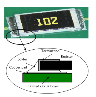
Figure 1 shows a photograph of a surface-mount resistor together with a diagram of it on a printed circuit board (PCB).
Figure 1: A photo and diagram of a typical surface-mounted resistor soldered to a PCB.
Table 1 shows the dimensions of the resistor and other key components in the model including the PCB.
35 μm
25 μm
105 μm
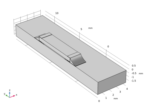
The simulation makes use of the symmetry so that it needs to include only half of the component (Figure 2). The modeling of the PCB is terminated a distance away from the resistor, in order to reduce effects of the boundary conditions.
Figure 2: The simulation models only one half of the resistor.
In operation, the resistor dissipates 0.2 W of power as heat. Conduction to the PCB and convection to the surrounding air provide cooling. In this model, the heat transfer occurs through conduction in the subdomains. The model simplifies the surface cooling and describes it using a heat transfer coefficient, h, in this case set to 10 W/(m2·K); the surrounding air temperature, Tinf, is at 300 K. The resulting heat transfer equation and boundary condition (included in the model using the Heat Transfer interface) are
where k is the thermal conductivity, and Q is the heating power per unit volume of the resistor (equal to 22.2 MW/m3 corresponding to 0.2 W in total).
The model handles thermal expansion using a static structural analysis using the Structural Mechanics interface (a description of the corresponding equations is available in the Structural Mechanics Module User’s Guide). The thermal and mechanical material properties in this model are taken from the material library. The data for the solid materials are temperature independent, and the reference values are shown in the table below.
E (GPa)
ν
α (ppm)
k (W/(m·K))
ρ (kg/m3)
Cp (J/(kg·K))
Air has temperature-dependent and pressure-dependent properties in the built-in material library. Because the temperature is a variable of the problem, it is automatically used. The pressure is by default set to 1 atm.
The stresses are zero at room temperature, 293 K. The boundary condition for the Solid Mechanics interface is that the cuts in the PCB do not rotate and have no net force normal to the cut.
Results and Discussion
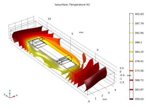
The isosurfaces in Figure 3 show the temperature distribution at steady state. The highest temperature occurs in the center of the resistor. The circuit board also heats up significantly.
Figure 3: Temperature distribution in the resistor and the circuit board at steady state.
Thermal stresses appear as a result of the temperature increase; they arise from the materials’ different expansion coefficients and from the bending of the PCB. Figure 4 plots the equivalent stress (von Mises) together with the resulting deformation of the assembly.
Figure 4: The thermally induced distribution of von Mises stress together with the deformation (magnified).
The highest stresses seem to occur in the termination material. It is interesting to compare these equivalent stresses to the yield stress and thereby investigate whether or not the material is irreversibly deformed. In that case the solder is the weak point. Figure 5 the stress in the solder alone.
Figure 5: Close-up of the von Mises stress in the solder joints.
The yield stress for solder is approximately 220 MPa. The highest equivalent stress appears to be about 40 percent of this value. The structure does not get permanently deformed directly when heated. However, it is possible that the solder displays creep strains over time because of the combination of fairly high stress levels and elevated temperatures.
Notes About the COMSOL Implementation
In this example, the Thermal Stress interface automatically adds and couples the Solid Mechanics interface and the Heat Transfer interface. This is done by the predefined multiphysics feature Thermal Expansion.
Build the geometry as an assembly of the bottom plate and the resistor to make it possible to mesh the parts independently. Use continuity conditions for the temperature and the displacements to connect the top and bottom parts of the geometry.
It is assumed that the temperature gradient in the normal direction on the cuts in the PCB is zero. The mechanical boundary conditions on the cuts must not impose a general state of compressive stress due to thermal expansion. At the same time, the restraint from the part of the PCB that is not modeled means that there is no rotation of the cross section. To obtain this effect, the entire cut must have the same (but unknown) displacement in the direction normal to the cut. This can be achieved by using a special setting in the Symmetry condition which allows a translation normal to the symmetry plane.
You solve the problem sequentially using two stationary study steps. The heat transfer problem is nonlinear because the air has temperature-dependent properties. The structural problem, on the other hand, is linear. For the structural analysis, use a memory-efficient iterative solver to make it possible to solve the problem also on computers with limited memory.
References
1. H. Lu, C. Bailey, M. Dusek, C. Hunt, and J. Nottay, “Modeling the Fatigue Life of Solder Joints of Surface Mount Resistors,” EMAP, 2000.
2. J.M. Coulson and J.F. Richardson, Chemical Engineering, vol. 1, Pergamon Press, appendix, 1990.
Application Library path: Heat_Transfer_Module/Thermal_Stress/surface_resistor
Modeling Instructions
From the File menu, choose New.
New
In the New window, click  Model Wizard.
Model Wizard
1
In the Model Wizard window, click  3D.
2
In the Select Physics tree, select Structural Mechanics>Thermal-Structure Interaction>Thermal Stress, Solid.
3
Click Add.
4
Click  Study.
5
In the Select Study tree, select General Studies>Stationary.
6
Global Definitions
Parameters 1
1
In the Model Builder window, under Global Definitions click Parameters 1.
2
In the Settings window for Parameters, locate the Parameters section.
3
Geometry 1
1
In the Model Builder window, under Component 1 (comp1) click Geometry 1.
2
In the Settings window for Geometry, locate the Units section.
3
From the Length unit list, choose mm.
Create the geometry. To simplify this step, insert a prepared 2D geometry sequence. On the Geometry toolbar, click Insert Sequence. Browse to the model’s Application Library folder and double-click the file surface_resistor.mph.
Work Plane 1 (wp1)>Union 1 (uni1)
The 2D geometry should now look as in the figure below.
Extrude 1 (ext1)
1
In the Geometry toolbar, click  Extrude.
2
3
In the Settings window for Extrude, locate the Distances section.
4
5
Click  Build All Objects.
Block 1 (blk1)
1
In the Geometry toolbar, click  Block.
2
In the Settings window for Block, locate the Size and Shape section.
3
In the Width text field, type 4.
4
In the Depth text field, type 16.
5
In the Height text field, type 1.6.
6
Locate the Position section. In the y text field, type -4.
7
In the z text field, type -1.6.
8
Click  Build All Objects.
9
Click the  Zoom Extents button in the Graphics toolbar.
Now, create an imprint of the resistor’s bottom boundary on the printed circuit board to make a pair with matching parts.
Form Union (fin)
1
In the Model Builder window, under Component 1 (comp1)>Geometry 1 click Form Union (fin).
2
In the Settings window for Form Union/Assembly, locate the Form Union/Assembly section.
3
From the Action list, choose Form an assembly.
4
Select the Create imprints check box.
5
In the Geometry toolbar, click  Build All.
The completed geometry is shown in Figure 2.
Add Material
1
In the Home toolbar, click  Add Material to open the Add Material window.
2
Go to the Add Material window.
3
In the tree, select Built-in>FR4 (Circuit Board).
4
Click Add to Component in the window toolbar.
5
In the tree, select Built-in>Alumina.
6
Click Add to Component in the window toolbar.
7
In the tree, select Built-in>Copper.
8
Click Add to Component in the window toolbar.
9
In the tree, select Material Library>Elements>Silver>Silver [solid].
10
Click Add to Component in the window toolbar.
11
In the tree, select Built-in>Solder, 60Sn-40Pb.
12
Click Add to Component in the window toolbar.
13
14
Click Add to Component in the window toolbar.
15
In the Home toolbar, click  Add Material to close the Add Material window.
Materials
FR4 (Circuit Board) (mat1)
1
In the Model Builder window, under Component 1 (comp1)>Materials click FR4 (Circuit Board) (mat1).
2
In the Settings window for Material, locate the Geometric Entity Selection section.
3
From the Selection list, choose Manual.
4
Click  Clear Selection.
5
Alumina (mat2)
1
In the Model Builder window, click Alumina (mat2).
2
Copper (mat3)
1
In the Model Builder window, click Copper (mat3).
2
Silver [solid] (mat4)
1
In the Model Builder window, click Silver [solid] (mat4).
2
Solder, 60Sn-40Pb (mat5)
1
In the Model Builder window, click Solder, 60Sn-40Pb (mat5).
2
Air (mat6)
1
In the Model Builder window, click Air (mat6).
2
Definitions
Symmetry Plane
1
In the Definitions toolbar, click  Box.
2
In the Settings window for Box, type Symmetry Plane in the Label text field.
3
Locate the Geometric Entity Level section. From the Level list, choose Boundary.
4
Locate the Box Limits section. In the x maximum text field, type 0.1.
5
Locate the Output Entities section. From the Include entity if list, choose Entity inside box.
Solid Mechanics (solid)
1
In the Model Builder window, under Component 1 (comp1) click Solid Mechanics (solid).
2
Symmetry 1
1
In the Physics toolbar, click  Boundaries and choose Symmetry.
2
In the Settings window for Symmetry, locate the Boundary Selection section.
3
From the Selection list, choose Symmetry Plane.
Continuity 1
1
In the Physics toolbar, click  Pairs and choose Continuity.
2
In the Settings window for Continuity, locate the Pair Selection section.
3
Under Pairs, click  Add.
4
In the Add dialog box, select Identity Boundary Pair 1 (ap1) in the Pairs list.
5
Roller 1
1
In the Physics toolbar, click  Boundaries and choose Roller.
2
Symmetry 2
1
In the Physics toolbar, click  Boundaries and choose Symmetry.
2
3
In the Settings window for Symmetry, click to expand the Normal Direction Condition section.
4
From the list, choose Free displacement.
Symmetry 3
1
In the Physics toolbar, click  Boundaries and choose Symmetry.
2
3
In the Settings window for Symmetry, locate the Normal Direction Condition section.
4
From the list, choose Free displacement.
Prescribed Displacement 1
1
In the Physics toolbar, click  Points and choose Prescribed Displacement.
2
3
In the Settings window for Prescribed Displacement, locate the Prescribed Displacement section.
4
Select the Prescribed in z direction check box.
Heat Transfer in Solids (ht)
In the Model Builder window, under Component 1 (comp1) click Heat Transfer in Solids (ht).
Fluid 1
1
In the Physics toolbar, click  Domains and choose Fluid.
2
Heat Source 1
1
In the Physics toolbar, click  Domains and choose Heat Source.
2
3
In the Settings window for Heat Source, locate the Heat Source section.
4
Click the Heat rate button.
5
In the P0 text field, type Psource.
Heat Flux 1
1
In the Physics toolbar, click  Boundaries and choose Heat Flux.
2
3
In the Settings window for Heat Flux, locate the Heat Flux section.
4
Click the Convective heat flux button.
5
In the h text field, type h_air.
6
In the Text text field, type T_air.
Next, add a continuity condition to the identity pair to couple the domains together.
Continuity 1
1
In the Physics toolbar, click  Pairs and choose Continuity.
2
In the Settings window for Continuity, locate the Pair Selection section.
3
Under Pairs, click  Add.
4
In the Add dialog box, select Identity Boundary Pair 1 (ap1) in the Pairs list.
5
Because the material properties are temperature dependent, the solution converges better if you supply an initial guess of the temperature.
Initial Values 1
1
In the Model Builder window, click Initial Values 1.
2
In the Settings window for Initial Values, locate the Initial Values section.
3
In the T text field, type T0.
Mesh 1
Free Triangular 1
1
In the Mesh toolbar, click  Boundary and choose Free Triangular.
2
Size 1
1
Right-click Free Triangular 1 and choose Size.
2
In the Settings window for Size, locate the Element Size section.
3
From the Predefined list, choose Fine.
4
Click the Custom button.
5
Locate the Element Size Parameters section. Select the Minimum element size check box.
6
7
Click  Build Selected.
Swept 1
1
In the Mesh toolbar, click  Swept.
2
In the Settings window for Swept, locate the Domain Selection section.
3
From the Geometric entity level list, choose Domain.
4
Distribution 1
1
In the Mesh toolbar, click  Distribution.
2
In the Settings window for Distribution, locate the Distribution section.
3
In the Number of elements text field, type 10.
4
Click  Build All.
Free Tetrahedral 1
In the Mesh toolbar, click  Free Tetrahedral.
Size 1
1
Right-click Free Tetrahedral 1 and choose Size.
2
In the Settings window for Size, locate the Geometric Entity Selection section.
3
From the Geometric entity level list, choose Boundary.
4
5
Locate the Element Size section. From the Predefined list, choose Extra fine.
6
Click  Build All.
Because the heat transfer problem is independent of the displacements, use the first stationary study step to find the temperature distribution and the second stationary step to solve for the displacements.
Study 1
Step 1: Stationary
1
In the Model Builder window, under Study 1 click Step 1: Stationary.
2
In the Settings window for Stationary, locate the Physics and Variables Selection section.
3
In the table, clear the Solve for check box for Solid Mechanics (solid).
Stationary 2
1
In the Study toolbar, click  Study Steps and choose Stationary>Stationary.
2
In the Settings window for Stationary, locate the Physics and Variables Selection section.
3
In the table, clear the Solve for check box for Heat Transfer in Solids (ht).
4
Click to expand the Values of Dependent Variables section. Find the Values of variables not solved for subsection. From the Settings list, choose User controlled.
5
From the Method list, choose Solution.
6
From the Study list, choose Study 1, Stationary.
7
In the Study toolbar, click  Compute.
Results
Surface 1
1
In the Model Builder window, expand the Stress (solid) node, then click Surface 1.
2
In the Settings window for Surface, locate the Expression section.
3
From the Unit list, choose MPa.
Hold down the left mouse button and drag in the Graphics window to rotate the geometry so that you see the opposite side of the resistor, which is where the largest stresses occur, as shown in Figure 4. Similarly, use the right mouse button to translate the geometry and the middle button to zoom.
Now, study the stresses in the solder.
Study 1/Solution 1 (3) (sol1)
In the Results toolbar, click  More Datasets and choose Solution.
Selection
1
In the Results toolbar, click  Attributes and choose Selection.
2
In the Settings window for Selection, locate the Geometric Entity Selection section.
3
From the Geometric entity level list, choose Domain.
4
Stress in Solder Joint
1
In the Results toolbar, click  3D Plot Group.
2
In the Settings window for 3D Plot Group, type Stress in Solder Joint in the Label text field.
3
Locate the Data section. From the Dataset list, choose Study 1/Solution 1 (3) (sol1).
4
Locate the Plot Settings section. Clear the Plot dataset edges check box.
Volume 1
1
Right-click Stress in Solder Joint and choose Volume.
2
In the Settings window for Volume, click Replace Expression in the upper-right corner of the Expression section. From the menu, choose Component 1 (comp1)>Solid Mechanics>Stress>solid.mises - von Mises stress - N/m².
3
Locate the Expression section. From the Unit list, choose MPa.
4
In the Stress in Solder Joint toolbar, click  Plot.
5
Click the  Go to YZ View button in the Graphics toolbar.
Compare the resulting plot with that in Figure 5.
Temperature (ht)
The second default plot group shows the temperature on the modeled geometry’s surface.
1
Click the  Go to Default View button in the Graphics toolbar.
Isothermal Contours (ht)
The third default plot shows the isosurfaces (Figure 3).