PDF

Heating Circuit
Introduction
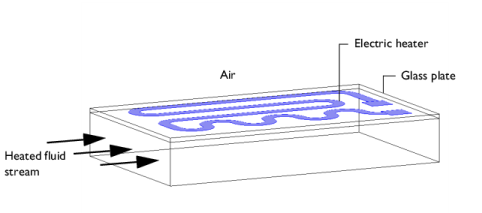
Small heating circuits find use in many applications. For example, in manufacturing processes they heat up reactive fluids. Figure 1 illustrates a typical heating device for this model. The device consists of an electrically resistive layer deposited on a glass plate. The layer causes Joule heating when a voltage is applied to the circuit. The layer’s properties determine the amount of heat produced.
Figure 1: Geometry of a heating device.
In this particular model, you must observe three important design considerations:
The heater must also work without failure. You achieve the first and second requirements by inserting a glass plate between the heating circuit and the fluid; it acts as a conducting separator. Glass is an ideal material for both these purposes because it is nonreactive and has a low coefficient of thermal expansion.
You must also avoid overheating due to the risk of self-ignition of the reactive fluid stream. Ignition is also the main reason for separating the electrical circuit from direct contact with the fluid. The heating device is tailored for each application, making virtual prototyping very important for manufacturers.
For heating circuits in general, detachment of the resistive layer often determines the failure rate. This is caused by excessive thermally induced interfacial stresses. Once the layer has detached, it gets locally overheated, which accelerates the detachment. Finally, in the worst case, the circuit might overheat and burn. From this perspective, it is also important to study the interfacial tension due to the different thermal-expansion coefficients of the resistive layer and the substrate as well as the differences in temperature. The geometric shape of the layer is a key parameter to design circuits for proper functioning. You can investigate all of the abovementioned aspects by modeling the circuit.
This multiphysics example simulates the electrical heat generation, the heat transfer, and the mechanical stresses and deformations of a heating circuit device. The model uses the Heat Transfer in Solids interface of the Heat Transfer Module in combination with the Electric Currents, Layered Shell interface from the AC/DC Module and the Solid Mechanics and Membrane interfaces from the Structural Mechanics Module.
Note: This model requires the AC/DC Module, Heat Transfer Module, and Structural Mechanics Module.
Model Definition
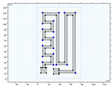
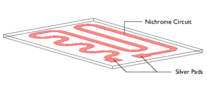
Figure 2 shows a drawing of the modeled heating circuit.
Figure 2: Drawing of the heating circuit deposited on a glass plate.
The device consists of a serpentine-shaped Nichrome resistive layer, 10 μm thick and 5 mm wide, deposited on a glass plate. At each end, it has a silver contact pad measuring 10 mm-by-10 mm-by-10 μm. When the circuit is in use, the deposited side of the glass plate is in contact with surrounding air, and the back side is in contact with the heated fluid. Assume that the edges and sides of the glass plate are thermally insulated.
Table 1 gives the resistor’s dimensions.
Table 1: Dimensions.
During operation the resistive layer produces heat. Model the electrically generated heat using the Electric Currents, Layered Shell interface from the AC/DC Module. An electric potential of 12 V is applied to the pads. In the model, you achieve this effect by setting the potential at one edge of the first pad to 12 V and that of one edge of the other pad to 0 V.
To model the heat transfer in the thin conducting layer, use the Thin Layer feature from the Heat Transfer in Solids interface. The heat rate per unit area (measured in W/m2) produced inside the thin layer is given by
(1)
where QDC = J · E = σ|∇tV|2 (W/m3) is the power density. The generated heat appears as an inward heat flux at the surface of the glass plate.
At steady state, the resistive layer dissipates the heat it generates in two ways: on its up side to the surrounding air (at 293 K), and on its down side to the glass plate. The glass plate is similarly cooled in two ways: on its circuit side by air, and on its back side by a process fluid (353 K). You model the heat fluxes to the surroundings using heat transfer coefficients, h. For the heat transfer to air, h = 5 W/(m2·K), representing natural convection. On the glass plate’s back side, h = 20 W/(m2·K), representing convective heat transfer to the fluid. The sides of the glass plate are insulated.
The model simulates thermal expansion using static structural-mechanics analyses. It uses the Solid Mechanics interface for the glass plate, and the Membrane interface for the circuit layer. The equations of these two interfaces are described in the Structural Mechanics Module User’s Guide. The stresses are set to zero at 293 K. You determine the boundary conditions for the Solid Mechanics interface by fixing one corner with respect to the x-, y-, and z-displacements and rotation.
Table 2 summarizes the material properties used in the model.
E [GPa]
ν
α [1/K]
k [W/(m·K)]
ρ [kg/m3]
Cp [J/(kg·K)]
Results and Discussion
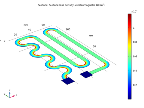
Figure 3 shows the heat that the resistive layer generates.
Figure 3: Stationary heat generation in the resistive layer when 12 V is applied.
The highest heating power occurs at the inner corners of the curves due to the higher current density at these spots. The total generated heat, as calculated by integration, is approximately 13.8 W.
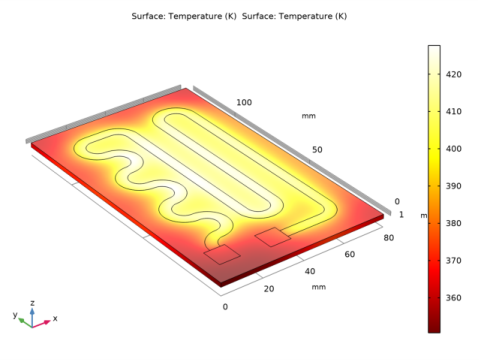
Figure 4 shows the temperature of the resistive layer and the glass plate at steady state.
Figure 4: Temperature distribution in the heating device at steady state.
The highest temperature is approximately 428 K, and it appears in the central section of the circuit layer. It is interesting to see that the differences in temperature between the fluid side and the circuit side of the glass plate are quite small because the plate is very thin. Using boundary integration, the integral heat flux on the fluid side evaluates to approximately 8.5 W. This means that the device transfers the majority of the heat it generates — 8.5 W out of 13.8 W — to the fluid, which is good from a design perspective, although the thermal resistance of the glass plate results in some losses.
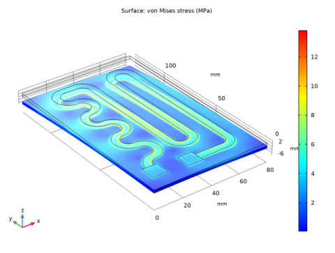
The temperature rise also induces thermal stresses due the materials’ different coefficients of thermal expansion. As a result, mechanical stresses and deformations arise in the layer and in the glass plate. Figure 5 shows the equivalent stress distribution in the device and the resulting deformations. During operation, the glass plate bends toward the air side.
Figure 5: The thermally induced von Mises stress plotted with the deformation.
The highest equivalent stress, approximately 13 MPa, occurs at the inner corners of the curves of the Nichrome circuit. The yield stress for high quality glass is roughly 250 MPa, and for Nichrome it is 360 MPa. This means that the individual objects remain structurally intact for the simulated heating power loads.
You must also consider stresses in the interface between the resistive layer and the glass plate. Assume that the yield stress of the surface adhesion in the interface is in the region of 50 MPa — a value significantly lower than the yield stresses of the other materials in the device. If the equivalent stress increases above this value, the resistive layer locally detaches from the glass. Once it has detached, heat transfer is locally impeded, which can lead to overheating of the resistive layer and eventually cause the device to fail.
Figure 6 displays the effective forces acting on the adhesive layer during heater operation. As the figure shows, the device experiences a maximum interfacial stress that is an order of magnitude smaller than the yield stress. This means that the device are OK in terms of adhesive stress.
Figure 6: The effective forces in the interface between the resistive layer and the glass plate.
Finally study the device’s deflections, shown in Figure 7.
Figure 7: Deviation from a plane surface on the fluid side of the glass plate.
The maximum deviation from being a planar surface, is approximately 50 μm. For high-precision applications, such as semiconductor processing, this might be a significant value that limits the device’s operating temperature.
Application Library path: Heat_Transfer_Module/Power_Electronics_and_Electronic_Cooling/heating_circuit
Modeling Instructions
From the File menu, choose New.
New
In the New window, click  Model Wizard.
Model Wizard
1
In the Model Wizard window, click  3D.
2
In the Select Physics tree, select Structural Mechanics>Thermal-Structure Interaction>Thermal Stress, Solid.
3
Click Add.
4
In the Select Physics tree, select AC/DC>Electric Fields and Currents>Electric Currents in Layered Shells (ecis).
5
Click Add.
6
In the Select Physics tree, select Structural Mechanics>Membrane (mbrn).
7
Click Add.
8
Click  Study.
9
In the Select Study tree, select General Studies>Stationary.
10
Geometry 1
The Thermal Stress interface includes Heat Transfer in Solids and Solid Mechanics. In the volume, these two interfaces solve for temperature and displacement, respectively. In the shell representing the circuit, the temperature, the electrical potential and displacement are solved by Heat Transfer In Solids, Electric Currents, Layered Shell, and Membrane interfaces, respectively.
Global Definitions
Parameters 1
1
In the Model Builder window, under Global Definitions click Parameters 1.
2
In the Settings window for Parameters, locate the Parameters section.
3
Geometry 1
1
In the Model Builder window, under Component 1 (comp1) click Geometry 1.
2
In the Settings window for Geometry, locate the Units section.
3
From the Length unit list, choose mm.
Block 1 (blk1)
1
In the Geometry toolbar, click  Block.
2
In the Settings window for Block, locate the Size and Shape section.
3
In the Width text field, type 80.
4
In the Depth text field, type 130.
5
In the Height text field, type 2.
6
Click  Build Selected.
Work Plane 1 (wp1)
1
In the Geometry toolbar, click  Work Plane.
2
In the Settings window for Work Plane, locate the Plane Definition section.
3
In the z-coordinate text field, type 2.
4
Click  Show Work Plane.
Work Plane 1 (wp1)>Plane Geometry
Click the  Zoom Extents button in the Graphics toolbar.
Work Plane 1 (wp1)>Square 1 (sq1)
1
In the Work Plane toolbar, click  Square.
2
In the Settings window for Square, locate the Size section.
3
In the Side length text field, type 10.
4
Locate the Position section. In the xw text field, type 7.
5
In the yw text field, type 10.
6
Click  Build Selected.
Work Plane 1 (wp1)>Square 2 (sq2)
1
Right-click Component 1 (comp1)>Geometry 1>Work Plane 1 (wp1)>Plane Geometry>Square 1 (sq1) and choose Duplicate.
2
In the Settings window for Square, locate the Position section.
3
In the xw text field, type 30.
4
In the yw text field, type 8.
5
Click  Build Selected.
Work Plane 1 (wp1)>Polygon 1 (pol1)
1
In the Work Plane toolbar, click  Polygon.
2
In the Settings window for Polygon, locate the Coordinates section.
3
From the Data source list, choose File.
4
Click Browse.
5
6
Click  Build Selected.
Work Plane 1 (wp1)>Fillet 1 (fil1)
1
In the Work Plane toolbar, click  Fillet.
2
On the object pol1, select Points 2–8, 23–29, 34, 36, 37, 41, and 42 only.
It might be easier to select the points by using the Selection List window. To open this window, in the Home toolbar click Windows and choose Selection List. (If you are running the cross-platform desktop, you find Windows in the main menu.)
3
In the Settings window for Fillet, locate the Radius section.
4
In the Radius text field, type 10.
5
Click  Build Selected.
Work Plane 1 (wp1)>Fillet 2 (fil2)
1
In the Work Plane toolbar, click  Fillet.
2
On the object fil1, select Points 6–12, 26–31, 37, 40, 43, 46, 49, and 50 only.
3
In the Settings window for Fillet, locate the Radius section.
4
In the Radius text field, type 5.
5
In the Work Plane toolbar, click  Build All.
Form Union (fin)
1
In the Home toolbar, click  Build All.
The geometry should look like the figure below.
Definitions
Add a selection that you can use later when applying boundary conditions and shell physics settings.
Circuit
1
In the Definitions toolbar, click  Explicit.
2
In the Settings window for Explicit, type Circuit in the Label text field.
3
Locate the Input Entities section. From the Geometric entity level list, choose Boundary.
4
Before creating the materials for use in this model, it is a good idea to specify which boundaries are to be modeled as conducting shells. Using this information, COMSOL Multiphysics can detect which material properties are needed.
Heat Transfer in Solids (ht)
Thin Layer 1
1
In the Model Builder window, under Component 1 (comp1) right-click Heat Transfer in Solids (ht) and choose Thin Structures>Thin Layer.
2
In the Settings window for Thin Layer, locate the Boundary Selection section.
3
From the Selection list, choose Circuit.
4
Locate the Layer Model section. From the Layer type list, choose Thermally thin approximation.
Electric Currents in Layered Shells (ecis)
1
In the Model Builder window, under Component 1 (comp1) click Electric Currents in Layered Shells (ecis).
2
In the Settings window for Electric Currents in Layered Shells, locate the Boundary Selection section.
3
From the Selection list, choose Circuit.
Conductive Shell 1
1
In the Model Builder window, under Component 1 (comp1)>Electric Currents in Layered Shells (ecis) click Conductive Shell 1.
2
In the Settings window for Conductive Shell, locate the Constitutive Relation D-E section.
3
From the εr list, choose User defined.
Use Layered Linear Elastic Material in membrane interface so that Layered Thermal Expansion multiphysics coupling can be used for modeling thermal effects.
Membrane (mbrn)
1
In the Model Builder window, under Component 1 (comp1) click Membrane (mbrn).
2
In the Settings window for Membrane, locate the Boundary Selection section.
3
From the Selection list, choose Circuit.
Layered Linear Elastic Material 1
1
In the Physics toolbar, click  Boundaries and choose Layered Linear Elastic Material.
2
In the Settings window for Layered Linear Elastic Material, locate the Boundary Selection section.
3
From the Selection list, choose Circuit.
Multiphysics
Layered Thermal Expansion 1 (tel1)
In the Physics toolbar, click  Multiphysics Couplings and choose Boundary>Layered Thermal Expansion.
Now set up the materials.
Add Material
1
In the Home toolbar, click  Add Material to open the Add Material window.
2
Go to the Add Material window.
3
In the tree, select Built-in>Silica glass.
4
Click Add to Component in the window toolbar.
5
In the Home toolbar, click  Add Material to close the Add Material window.
Materials
Silver Layer
1
In the Model Builder window, under Component 1 (comp1) right-click Materials and choose Layers>Single Layer Material.
2
In the Settings window for Material, type Silver Layer in the Label text field.
3
Locate the Geometric Entity Selection section. From the Selection list, choose Circuit.
4
Locate the Orientation and Position section. From the Position list, choose Downside on boundary.
5
Locate the Material Contents section. In the table, enter the following settings:
Nichrome Layer
1
Right-click Materials and choose Layers>Single Layer Material.
2
3
In the Settings window for Material, type Nichrome Layer in the Label text field.
4
Locate the Orientation and Position section. From the Position list, choose Downside on boundary.
5
Locate the Material Contents section. In the table, enter the following settings:
Electric Currents in Layered Shells (ecis)
In the Model Builder window, under Component 1 (comp1) click Electric Currents in Layered Shells (ecis).
Ground 1
1
In the Physics toolbar, click  Edges and choose Ground.
2
Electric Potential 1
1
In the Physics toolbar, click  Edges and choose Electric Potential.
2
3
In the Settings window for Electric Potential, locate the Electric Potential section.
4
In the V0 text field, type V_in.
Continuity 1
1
In the Physics toolbar, click  Edges and choose Continuity.
2
In the Settings window for Continuity, locate the Layer Selection section.
3
From the Source list, choose Silver Layer (mat2).
4
From the Destination list, choose Nichrome Layer (mat3).
With the materials defined, set up the remaining physics of the model. In the next section, the resistive loss within the circuit is defined as a heat source for the thermal stress physics. The resistive loss is calculated automatically within the Electric Currents, Layered Shell physics interface. Add the coupling feature Electromagnetic Heating to take the resistive loss into account.
Multiphysics
Electromagnetic Heating, Layered Shell 1 (ehls1)
In the Physics toolbar, click  Multiphysics Couplings and choose Boundary>Electromagnetic Heating, Layered Shell.
Add the coupling feature Solid-Shell Connection to connect the Solid Mechanics with Membrane.
Solid-Thin Structure Connection 1 (sshc1)
In the Physics toolbar, click  Multiphysics Couplings and choose Global>Solid-Thin Structure Connection.
Heat Transfer in Solids (ht)
In the Model Builder window, under Component 1 (comp1) click Heat Transfer in Solids (ht).
Heat Flux 1
1
In the Physics toolbar, click  Boundaries and choose Heat Flux.
2
3
In the Settings window for Heat Flux, locate the Heat Flux section.
4
Click the Convective heat flux button.
5
In the h text field, type h_air.
6
In the Text text field, type T_air.
Heat Flux 2
1
In the Physics toolbar, click  Boundaries and choose Heat Flux.
2
3
In the Settings window for Heat Flux, locate the Heat Flux section.
4
Click the Convective heat flux button.
5
In the h text field, type h_fluid.
6
In the Text text field, type T_fluid.
Solid Mechanics (solid)
In order for the problem to be well posed, the glass plate must be constrained so that it does not have any possible rigid body translations or rotations. The constraints must be such that no stresses are induced by inhibited thermal expansion.
1
In the Model Builder window, under Component 1 (comp1) click Solid Mechanics (solid).
Rigid Motion Suppression 1
1
In the Physics toolbar, click  Domains and choose Rigid Motion Suppression.
2
Mesh 1
Free Triangular 1
1
In the Mesh toolbar, click  Boundary and choose Free Triangular.
2
Size 1
1
Right-click Free Triangular 1 and choose Size.
2
In the Settings window for Size, locate the Geometric Entity Selection section.
3
From the Selection list, choose Circuit.
4
Locate the Element Size section. Click the Custom button.
5
Locate the Element Size Parameters section. Select the Maximum element size check box.
6
Swept 1
In the Mesh toolbar, click  Swept.
Distribution 1
1
In the Mesh toolbar, click  Distribution.
2
In the Settings window for Distribution, locate the Distribution section.
3
In the Number of elements text field, type 3.
4
Click  Build All.
Study 1
In order to improve the solver’s performance, set the scaling of Solid Mechanics degree of freedom to 1e-3.
Solution 1 (sol1)
1
In the Study toolbar, click  Show Default Solver.
2
In the Model Builder window, expand the Solution 1 (sol1) node.
3
In the Model Builder window, expand the Study 1>Solver Configurations>Solution 1 (sol1)>Dependent Variables 1 node, then click Displacement field (comp1.u).
4
In the Settings window for Field, locate the Scaling section.
5
From the Method list, choose Manual.
6
In the Scale text field, type 1e-3.
7
In the Model Builder window, under Study 1>Solver Configurations>Solution 1 (sol1)>Dependent Variables 1 click Displacement field (comp1.u2).
8
In the Settings window for Field, locate the Scaling section.
9
In the Scale text field, type 1e-3.
10
In the Study toolbar, click  Compute.
Results
The default plots show the von Mises stress including the deformation (Figure 5) and the temperature (Figure 4) on the surface of the full 3D geometry, and the electric potential and the von Mises stress on the circuit layer.
Surface 1
1
In the Model Builder window, expand the Results>Stress (solid) node, then click Surface 1.
2
In the Settings window for Surface, locate the Expression section.
3
From the Unit list, choose MPa.
4
In the Stress (solid) toolbar, click  Plot.
Surface 1
1
In the Model Builder window, expand the Results>Stress (mbrn) node, then click Surface 1.
2
In the Settings window for Surface, locate the Expression section.
3
From the Unit list, choose MPa.
4
In the Stress (mbrn) toolbar, click  Plot.
Study 1/Solution 1 (2) (sol1)
1
In the Model Builder window, expand the Results>Datasets node.
2
Right-click Results>Datasets>Study 1/Solution 1 (sol1) and choose Duplicate.
Selection
1
In the Results toolbar, click  Attributes and choose Selection.
2
In the Settings window for Selection, locate the Geometric Entity Selection section.
3
From the Geometric entity level list, choose Boundary.
4
From the Selection list, choose Circuit.
To generate Figure 3 follow the steps below.
Surface Losses
1
In the Results toolbar, click  3D Plot Group.
2
In the Settings window for 3D Plot Group, type Surface Losses in the Label text field.
3
Locate the Data section. From the Dataset list, choose Study 1/Solution 1 (2) (sol1).
Surface 1
1
In the Surface Losses toolbar, click  Surface.
2
In the Settings window for Surface, click Replace Expression in the upper-right corner of the Expression section. From the menu, choose Component 1 (comp1)>Electric Currents in Layered Shells>Heating and losses>ecis.Qsh - Surface loss density, electromagnetic - W/m².
3
In the Surface Losses toolbar, click  Plot.
4
Click the  Scene Light button in the Graphics toolbar.
5
Click the  Zoom Extents button in the Graphics toolbar.
The following steps generate a plot of the norm of the surface traction vector in the surface plane (see Figure 6):
Interface Stress
1
In the Home toolbar, click  Add Plot Group and choose 3D Plot Group.
2
In the Settings window for 3D Plot Group, type Interface Stress in the Label text field.
3
Locate the Data section. From the Dataset list, choose Study 1/Solution 1 (2) (sol1).
Surface 1
1
In the Interface Stress toolbar, click  Surface.
2
In the Settings window for Surface, locate the Expression section.
3
In the Expression text field, type sqrt(solid.Tax^2+solid.Tay^2).
4
From the Unit list, choose MPa.
5
In the Interface Stress toolbar, click  Plot.
Finally, to obtain Figure 7, proceed as follows:
6
In the Results toolbar, click  More Datasets and choose Surface.
Surface 1
Select Boundary 3 only.
Displacement, Bottom Boundary
1
In the Results toolbar, click  2D Plot Group.
2
In the Settings window for 2D Plot Group, type Displacement, Bottom Boundary in the Label text field.
Surface 1
1
Right-click Displacement, Bottom Boundary and choose Surface.
2
In the Settings window for Surface, click Replace Expression in the upper-right corner of the Expression section. From the menu, choose Component 1 (comp1)>Solid Mechanics>Displacement>solid.disp - Displacement magnitude - m.
3
Locate the Expression section. In the Unit field, type um.
4
In the Displacement, Bottom Boundary toolbar, click  Plot.
The absolute displacement is not important in itself, since it is just a function of how the rigid body constraints are applied. Instead, you want to see how much the boundary deviates from being planar. To display that, create a linear approximation to the deformation using a least-squares fit. Then, plot the deviation from that plane.
Definitions (comp1)
Integration 1 (intop1)
1
In the Definitions toolbar, click  Nonlocal Couplings and choose Integration.
2
In the Settings window for Integration, type intBelow in the Operator name text field.
3
Locate the Source Selection section. From the Geometric entity level list, choose Boundary.
4
5
Locate the Advanced section. From the Frame list, choose Material  (X, Y, Z).
Variables 1
1
In the Model Builder window, right-click Definitions and choose Variables.
2
In the Settings window for Variables, locate the Variables section.
3
Click  Load from File.
4
5
Click the  Show More Options button in the Model Builder toolbar.
6
In the Show More Options dialog box, in the tree, select the check box for the node General>Variable Utilities.
7
Matrix Inverse 1 (matinv1)
1
In the Definitions toolbar, click  Variable Utilities and choose Matrix Inverse.
2
In the Settings window for Matrix Inverse, type AInv in the Name text field.
3
Locate the Input Matrix section. From the Matrix format list, choose Symmetric.
4
Study 1
In the Study toolbar, click  Update Solution.
Results
Surface 1
1
In the Model Builder window, under Results>Displacement, Bottom Boundary click Surface 1.
2
In the Settings window for Surface, locate the Expression section.
3
In the Expression text field, type w-(w_0+w_x*X+w_y*Y).
4
In the Displacement, Bottom Boundary toolbar, click  Plot.
To calculate the values for the total generated heat and the integrated heat flux on the fluid side, perform a boundary integration:
Surface Integration 1
1
In the Results toolbar, click  More Derived Values and choose Integration>Surface Integration.
2
3
In the Settings window for Surface Integration, click Replace Expression in the upper-right corner of the Expressions section. From the menu, choose Component 1 (comp1)>Heat Transfer in Solids>Boundary fluxes>ht.q0 - Inward heat flux - W/m².
4
Click  Evaluate.
Table
1
Go to the Table window.
The result should be close to 8.5 W.
Results
Surface Integration 2
1
In the Results toolbar, click  More Derived Values and choose Integration>Surface Integration.
2
In the Settings window for Surface Integration, locate the Selection section.
3
From the Selection list, choose Circuit.
4
Click Replace Expression in the upper-right corner of the Expressions section. From the menu, choose Component 1 (comp1)>Electric Currents in Layered Shells>Heating and losses>ecis.Qsh - Surface loss density, electromagnetic - W/m².
5
Click  Evaluate.
Table
1
Go to the Table window.
The result should be close to 13.8 W.