PDF

Disk-Stack Heat Sink
Introduction
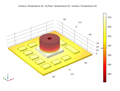
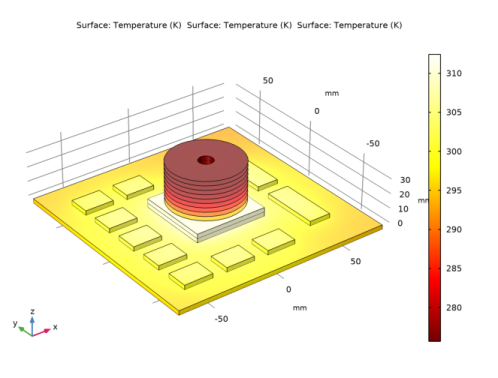
This example studies the cooling effects of a disk-stack heat sink on an electronic component. The heat sink shape (see Figure 1) shows several thin aluminum disks piled up around a central hollow column. Such a configuration allows cooling of large surfaces of aluminum fins by air at ambient temperature.
Figure 1: Steady-state surface temperature distribution of the electronic device.
To evaluate the efficiency of the heat sink, this tutorial follows a typical preliminary board-level thermal analysis. First, a simulation of the board with some Integrated Circuits (ICs) is performed. Then, the disk-stack heat sink is added above the main hot electronic component to observe cooling effects. The final part adds a copper layer to the bottom of the board in order to obtain a more uniform temperature distribution and see how it affects the heat transfer in the circuit board.
This exercise highlights a number of important modeling techniques such as combining 3D solids and shells and using thin layer boundary conditions when replacing 3D thin geometries by 2D boundaries.
Model Definition
Geometry
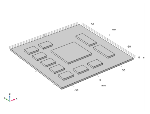
Figure 2 shows that the first studied geometry is made of a circuit board with several ICs on it.
Figure 2: First geometry without heat sink.
This typical board-level thermal analysis determines the temperature profile in and around a high-power chip. The printed-circuit board usually consists of multiple layers of FR4 material (Flame Resistant 4) and copper traces along the board. Hence, the thermal conductivity along the board is much higher than the conductivity through it. It is possible to take several approaches for simulating such a board in COMSOL Multiphysics. This example uses a macro-level approach and assumes a homogeneous PC board with anisotropic thermal material properties. In this case, the heat diffusion through the board and the one lost due to natural convection is insufficient to adequately cool the chip. Hence, a disk-stack heat sink is required to increase the effective cooling area for the chip.
Regarding materials
The IC packages and the PC board on which they are mounted must be defined. In reality, these components have very detailed structures and are made of a variety of materials. For a board-level analysis such as the present one, though, it is much simpler to lump all these detailed structures into single homogeneous materials for each component, instead of accounting for the thermal characteristics of a multilayer PC board, which typically consist of multiple layers of FR4 (insulator) interspersed with layers of copper traces. The thermal result of this construction is that the thermal conductivity along the board is considerably higher than through it. Physical property values depend on the number of layers, how dense the lines are, and how many vias (interconnections between layers) per unit area are present. The numbers in an estimate for a highly layered board which are used to create a strong difference in conductivity between the printed-circuit board plane (xy) and the orthogonal direction z. Those properties are presented in Table 1. The units are W/(m·K) for thermal conductivity, kg/m3 for density and J/(kg·K) for heat capacity.
Thermal configuration
In this problem the large central chip dissipates 20 W, the array of smaller chips are 1 W each, and the two elongated chips are 2 W each. The volumetric heat source is calculated by dividing the heat power by the volume of the considered IC.
In this example, you assume that a fan cools the board, and specify a convective heat transfer coefficient for the boundary heat flux. Here, you look for a preliminary sizing calculation and simply assume a convective coefficient, h, of 20 W/(m2·K). This corresponds to a fan blowing air at approximately 1 m/s on a plate. The air temperature is set to T0 = 273.15 K during the whole modeling process.
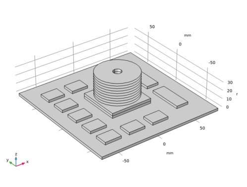
Without a heat sink, the temperature rise in the main chip is higher than the maximum operating temperature. A stacked disk heat sink increases the effective area and therefore cools the chip further. This heat sink consists of a series of thin disks supported by a central hollow column that is mounted to the chip with an aluminum base corresponding to the size of the chip. The heat sink is mounted dry and must therefore account for contact resistance. Figure 3 shows the new geometry with the main chip equipped with the heat sink.
Figure 3: Full geometry of the PC board equipped with the heat sink.
Thermal linkage between the IC and the added heat sink is made using the Thermal Contact boundary condition. It provides a heat transfer coefficient at the two surfaces in contact according to (1.9 in Ref. 1):
This expression involves two parameters related to the surface microscopic asperities: σ, the average asperities height, and m, the average asperities slope. In this case, σ and m are set to 1 μm and 0.5, respectively. The microhardness of the softer material, Hc, is here the hardness of aluminum, equal to 165 MPa. The contact pressure, p, is set to 20 kPa. The thermal conductivity kgap is related to the material in the interstitial gap, here assumed to be air at atmospheric pressure. It is equal to 0.025 W/(m·K).
A design value of 0.3 mm is chosen for the thickness of the fins and the central hollow column.
Finally, the last part explores the possibility of evening out the temperature distribution across the PC board. For instance, add a 0.4 mm layer of copper across the board entire bottom surface. The previous cross section does not suggest much success for this approach. However, it is interesting to check such an analysis for the sake of comparison. In COMSOL Multiphysics, this is easily done using the Thin Layer boundary condition.
Results and Discussion
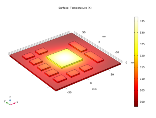
Figure 4 shows the stationary temperature field on the surfaces of the board and chips in kelvin. The central region of the IC becomes rather hot (337 K) and needs extra cooling.
Figure 4: Temperature distribution of the PC board without the heat sink.
As Figure 5 shows, there is a steep thermal gradient between the IC and the heat sink base which is caused by the contact resistance and the significant cooling by the heat sink fins. The maximum device temperature has now dropped to 313 K, which is 24 K lower than without the heat sink.
Figure 5: Temperature distribution of the PC board with its heat sink.
Finally, Figure 6 shows that adding a layer of copper at the bottom of the Circuit Board is ineffective. This phenomenon agrees with the fact that the Circuit Board material has a rather poor thermal conductivity along the vertical z-axis (orthogonal to the PC plane).
Figure 6: Temperature distribution of the PC board with its heat sink and a layer of copper at bottom
Notes About the COMSOL Implementation
In this application, use the Heat Transfer in Thin Shells interface to model thermal behavior of fins. The number of elements is significantly reduced because, instead of creating a thin 3D geometry, only a 2D layer is meshed.
References
1. A.D. Kraus and A. Bejan, Heat Transfer Handbook, John Wiley & Sons, 2003.
Application Library path: Heat_Transfer_Module/Thermal_Contact_and_Friction/disk_stack_heat_sink
Modeling Instructions
From the File menu, choose New.
New
In the New window, click  Model Wizard.
Model Wizard
1
In the Model Wizard window, click  3D.
2
In the Select Physics tree, select Heat Transfer>Heat Transfer in Solids (ht).
3
Click Add.
4
Click  Study.
5
In the Select Study tree, select General Studies>Stationary.
6
Global Definitions
Parameters 1
1
In the Model Builder window, under Global Definitions click Parameters 1.
2
In the Settings window for Parameters, locate the Parameters section.
3
Click  Load from File.
4
Geometry 1
1
In the Model Builder window, under Component 1 (comp1) click Geometry 1.
2
In the Settings window for Geometry, locate the Units section.
3
From the Length unit list, choose mm.
Block 1 (blk1)
1
In the Geometry toolbar, click  Block.
2
In the Settings window for Block, locate the Size and Shape section.
3
In the Width text field, type CB_w.
4
In the Depth text field, type CB_l.
5
In the Height text field, type CB_t.
6
Locate the Position section. In the x text field, type -CB_w/2.
7
In the y text field, type -CB_l/2.
8
In the z text field, type -CB_t.
9
Click  Build Selected.
Block 2 (blk2)
1
In the Geometry toolbar, click  Block.
2
In the Settings window for Block, locate the Size and Shape section.
3
In the Width text field, type IC1_w.
4
In the Depth text field, type IC1_l.
5
In the Height text field, type IC1_t.
6
Locate the Position section. In the x text field, type -CB_w/2+IC1_w.
7
In the y text field, type -CB_l/2+IC1_l.
8
Click  Build Selected.
Block 3 (blk3)
1
In the Geometry toolbar, click  Block.
2
In the Settings window for Block, locate the Size and Shape section.
3
In the Width text field, type IC2_l.
4
In the Depth text field, type IC2_w.
5
In the Height text field, type IC2_t.
6
Locate the Position section. In the x text field, type -60.
7
In the y text field, type -60.
8
Click  Build Selected.
Copy 1 (copy1)
1
In the Geometry toolbar, click  Transforms and choose Copy.
2
3
In the Settings window for Copy, locate the Displacement section.
4
In the x text field, type 0 0 0 0 range(30,30,60) 30.
5
In the y text field, type range(25, 25, 100) 0 0 100.
6
Click  Build Selected.
Block 4 (blk4)
1
In the Geometry toolbar, click  Block.
2
In the Settings window for Block, locate the Size and Shape section.
3
In the Width text field, type IC3_w.
4
In the Depth text field, type IC3_l.
5
In the Height text field, type IC3_t.
6
Locate the Position section. In the x text field, type 40.
7
In the y text field, type -50.
8
Click  Build Selected.
Copy 2 (copy2)
1
In the Geometry toolbar, click  Transforms and choose Copy.
2
3
In the Settings window for Copy, locate the Displacement section.
4
In the y text field, type 50.
5
In the Geometry toolbar, click  Build All.
Definitions
ICs, Type 1
1
In the Definitions toolbar, click  Explicit.
2
In the Settings window for Explicit, type ICs, Type 1 in the Label text field.
3
It might be easier to select the correct domain by using the Selection List window. To open this window, in the Home toolbar click Windows and choose Selection List. (If you are running the cross-platform desktop, you find Windows in the main menu.)
ICs, Type 2
1
In the Definitions toolbar, click  Explicit.
2
In the Settings window for Explicit, type ICs, Type 2 in the Label text field.
3
ICs, Type 3
1
In the Definitions toolbar, click  Explicit.
2
In the Settings window for Explicit, type ICs, Type 3 in the Label text field.
3
ICs
1
In the Definitions toolbar, click  Union.
2
In the Settings window for Union, type ICs in the Label text field.
3
Locate the Input Entities section. Under Selections to add, click  Add.
4
In the Add dialog box, select ICs, Type 1 in the Selections to add list.
5
6
In the Settings window for Union, locate the Input Entities section.
7
Under Selections to add, click  Add.
8
In the Add dialog box, select ICs, Type 2 in the Selections to add list.
9
10
In the Settings window for Union, locate the Input Entities section.
11
Under Selections to add, click  Add.
12
In the Add dialog box, select ICs, Type 3 in the Selections to add list.
13
Add Material
1
In the Home toolbar, click  Add Material to open the Add Material window.
2
Go to the Add Material window.
3
In the tree, select Built-in>Silica glass.
4
Click Add to Component in the window toolbar.
5
In the tree, select Built-in>FR4 (Circuit Board).
6
Click Add to Component in the window toolbar.
7
In the Home toolbar, click  Add Material to close the Add Material window.
Materials
Silica glass (mat1)
1
In the Model Builder window, under Component 1 (comp1)>Materials click Silica glass (mat1).
2
In the Settings window for Material, locate the Geometric Entity Selection section.
3
From the Selection list, choose ICs.
FR4 (Circuit Board) (mat2)
1
In the Model Builder window, click FR4 (Circuit Board) (mat2).
2
Here, the PC board needs to have an orthotropic thermal conductivity to account for conduction induced by several copper tracks in the xy-planes of the board.
3
In the Settings window for Material, locate the Material Contents section.
4
Heat Transfer in Solids (ht)
Initial Values 1
1
In the Model Builder window, under Component 1 (comp1)>Heat Transfer in Solids (ht) click Initial Values 1.
2
In the Settings window for Initial Values, locate the Initial Values section.
3
In the T text field, type T0.
Heat Source 1
1
In the Physics toolbar, click  Domains and choose Heat Source.
2
In the Settings window for Heat Source, locate the Domain Selection section.
3
From the Selection list, choose ICs, Type 1.
4
Locate the Heat Source section. Click the Heat rate button.
5
In the P0 text field, type P1.
Heat Source 2
1
In the Physics toolbar, click  Domains and choose Heat Source.
2
In the Settings window for Heat Source, locate the Domain Selection section.
3
From the Selection list, choose ICs, Type 2.
4
Locate the Heat Source section. Click the Heat rate button.
5
In the P0 text field, type P2*8.
Heat Source 3
1
In the Physics toolbar, click  Domains and choose Heat Source.
2
In the Settings window for Heat Source, locate the Domain Selection section.
3
From the Selection list, choose ICs, Type 3.
4
Locate the Heat Source section. Click the Heat rate button.
5
In the P0 text field, type P3*2.
Heat Flux 1
1
In the Physics toolbar, click  Boundaries and choose Heat Flux.
2
In the Settings window for Heat Flux, locate the Heat Flux section.
3
Click the Convective heat flux button.
4
In the h text field, type htc.
5
In the Text text field, type T0.
In the followings, select boundaries 1 to 72. For more convenience, use the Paste Selection button.
6
Locate the Boundary Selection section. Click  Paste Selection.
7
In the Paste Selection dialog box, type 1-72 in the Selection text field.
8
Study 1
In the Home toolbar, click  Compute.
Results
Temperature (ht)
This is the first temperature distribution. It clearly outlines that the main chip needs more efficient cooling. This is the aim of the next part in which a disk-stack heat sink will be added on the top of the central chip.
Geometry 1
Block 5 (blk5)
1
In the Geometry toolbar, click  Block.
2
In the Settings window for Block, locate the Size and Shape section.
3
In the Width text field, type IC1_w.
4
In the Depth text field, type IC1_l.
5
In the Height text field, type IC1_t.
6
Locate the Position section. In the x text field, type -CB_w/2+IC1_w.
7
In the y text field, type -CB_l/2+IC1_l.
8
In the z text field, type IC1_t.
9
Click  Build Selected.
Cylinder 1 (cyl1)
1
In the Geometry toolbar, click  Cylinder.
2
In the Settings window for Cylinder, locate the Object Type section.
3
From the Type list, choose Surface.
4
Locate the Size and Shape section. In the Radius text field, type i_radius.
5
In the Height text field, type t_h.
6
Locate the Position section. In the z text field, type IC1_t*2.
7
Locate the Selections of Resulting Entities section. Find the Cumulative selection subsection. Click New.
8
In the New Cumulative Selection dialog box, type Fins in the Name text field.
9
10
In the Settings window for Cylinder, click  Build Selected.
Work Plane 1 (wp1)
1
In the Geometry toolbar, click  Work Plane.
2
In the Settings window for Work Plane, locate the Plane Definition section.
3
From the Plane type list, choose Face parallel.
4
On the object blk5, select Boundary 4 only.
5
In the Offset in normal direction text field, type air_sp.
6
Click  Show Work Plane.
Work Plane 1 (wp1)>Circle 1 (c1)
1
In the Work Plane toolbar, click  Circle.
2
In the Settings window for Circle, locate the Size and Shape section.
3
In the Radius text field, type i_radius.
4
Click  Build Selected.
5
Click the  Zoom Extents button in the Graphics toolbar.
Work Plane 1 (wp1)>Circle 2 (c2)
1
In the Work Plane toolbar, click  Circle.
2
In the Settings window for Circle, locate the Size and Shape section.
3
In the Radius text field, type o_radius.
4
Click  Build Selected.
5
Click the  Zoom Extents button in the Graphics toolbar.
Work Plane 1 (wp1)>Difference 1 (dif1)
1
In the Work Plane toolbar, click  Booleans and Partitions and choose Difference.
2
3
In the Settings window for Difference, locate the Difference section.
4
Find the Objects to subtract subsection. Select the  Activate Selection toggle button.
5
6
Click  Build Selected.
Work Plane 1 (wp1)
1
In the Model Builder window, click Work Plane 1 (wp1).
2
In the Settings window for Work Plane, locate the Selections of Resulting Entities section.
3
Find the Cumulative selection subsection. From the Contribute to list, choose Fins.
4
Click  Build Selected.
Array 1 (arr1)
1
In the Geometry toolbar, click  Transforms and choose Array.
2
3
In the Settings window for Array, locate the Size section.
4
From the Array type list, choose Linear.
5
In the Size text field, type n_fins.
6
Locate the Displacement section. In the z text field, type air_sp.
7
Locate the Selections of Resulting Entities section. Find the Cumulative selection subsection. From the Contribute to list, choose Fins.
8
In the Geometry toolbar, click  Build All.
Add Material
1
In the Home toolbar, click  Add Material to open the Add Material window.
2
Go to the Add Material window.
3
In the tree, select Built-in>Aluminum.
4
Click Add to Component in the window toolbar.
5
In the tree, select Built-in>Aluminum.
6
Click Add to Component in the window toolbar.
7
In the Home toolbar, click  Add Material to close the Add Material window.
Materials
Aluminum (mat3)
1
In the Model Builder window, under Component 1 (comp1)>Materials click Aluminum (mat3).
2
Aluminum Fins
1
In the Model Builder window, under Component 1 (comp1)>Materials click Aluminum 1 (mat4).
2
In the Settings window for Material, type Aluminum Fins in the Label text field.
3
Locate the Geometric Entity Selection section. From the Geometric entity level list, choose Boundary.
4
From the Selection list, choose Fins.
It is necessary to add a second Aluminum material since the first one is used on a different geometric-entity level.
Heat Transfer in Solids (ht)
Heat Flux 1
Add the newly created external boundaries of the heat sink base.
1
In the Model Builder window, under Component 1 (comp1)>Heat Transfer in Solids (ht) click Heat Flux 1.
2
In the Settings window for Heat Flux, locate the Boundary Selection section.
3
Click  Paste Selection.
4
In the Paste Selection dialog box, type 49 50 52 64 115 in the Selection text field.
5
Thermal Contact 1
1
In the Physics toolbar, click  Boundaries and choose Thermal Contact.
2
In the Settings window for Thermal Contact, locate the Boundary Selection section.
3
Click  Paste Selection.
4
In the Paste Selection dialog box, type 51 in the Selection text field.
5
6
In the Settings window for Thermal Contact, locate the Thermal Contact section.
7
From the hg list, choose Parallel-plate gap gas conductance.
8
Locate the Contact Surface Properties section. In the p text field, type 20[kPa].
9
In the Hc text field, type 165[MPa].
10
Click to expand the Gap Properties section. From the kgap list, choose User defined.
Add Physics
1
In the Physics toolbar, click  Add Physics to open the Add Physics window.
2
Go to the Add Physics window.
3
In the tree, select Heat Transfer>Thin Structures>Heat Transfer in Shells (htlsh).
4
Click to expand the Dependent Variables section. In the Temperature text field, type T.
A new physics interface is required here to take into account out-of-plane convective cooling. In the physics interface selection, you have to use the same temperature variable, T, to couple the two physics interfaces.
5
Click Add to Component 1 in the window toolbar.
6
In the Physics toolbar, click  Add Physics to close the Add Physics window.
Heat Transfer in Shells (htlsh)
1
In the Settings window for Heat Transfer in Shells, locate the Boundary Selection section.
2
From the Selection list, choose Fins.
Heat Flux, Interface 1
1
Right-click Component 1 (comp1)>Heat Transfer in Shells (htlsh) and choose Interfaces>Heat Flux, Interface.
2
In the Settings window for Heat Flux, Interface, locate the Boundary Selection section.
3
From the Selection list, choose Fins.
4
Locate the Heat Flux section. Click the Convective heat flux button.
5
In the h text field, type htc.
6
In the Text text field, type T0.
Materials
Aluminum Fins (mat4)
1
In the Model Builder window, under Component 1 (comp1)>Materials click Aluminum Fins (mat4).
2
In the Settings window for Material, locate the Material Contents section.
3
Add Study
1
In the Home toolbar, click  Add Study to open the Add Study window.
2
Go to the Add Study window.
3
Find the Studies subsection. In the Select Study tree, select General Studies>Stationary.
4
Click  Add Study.
5
In the Home toolbar, click  Add Study to close the Add Study window.
Study 2
In the Home toolbar, click  Compute.
Results
Temperature (ht) 1
In the Model Builder window, expand the Results>Temperature (ht) 1 node.
Selection 1
1
In the Model Builder window, expand the Results>Temperature (ht) 1>Surface 1 node, then click Selection 1.
2
In the Settings window for Selection, locate the Selection section.
3
From the Selection list, choose All boundaries.
Temperature (ht) 1
1
In the Model Builder window, click Temperature (ht) 1.
2
In the Temperature (ht) 1 toolbar, click  Plot.
This is the temperature profile once the heat sink has been added. The heat sink significantly reduces the average temperature of the main chip.
Add Material
1
In the Home toolbar, click  Add Material to open the Add Material window.
2
Go to the Add Material window.
3
In the tree, select Built-in>Copper.
4
Click Add to Component in the window toolbar.
5
In the Home toolbar, click  Add Material to close the Add Material window.
Heat Transfer in Solids (ht)
In the Model Builder window, under Component 1 (comp1) click Heat Transfer in Solids (ht).
Thin Layer 1
1
In the Physics toolbar, click  Boundaries and choose Thin Layer.
2
In the Settings window for Thin Layer, locate the Layer Model section.
3
From the Layer type list, choose Thermally thin approximation.
4
Materials
Copper (mat5)
1
In the Model Builder window, under Component 1 (comp1)>Materials click Copper (mat5).
2
In the Settings window for Material, locate the Geometric Entity Selection section.
3
From the Geometric entity level list, choose Boundary.
4
5
Locate the Material Contents section. In the table, enter the following settings:
Study 2
In the Home toolbar, click  Compute.
Results
Temperature (ht) 1
This is the temperature profile once the copper layer has been added. No significant effect due to this modification can be observed.
In order to visualize the temperature on each side of the thermal contact, follow the next steps.
Temperature (ht) 1.1
Right-click Temperature (ht) 1 and choose Duplicate.
Surface 2
In the Model Builder window, right-click Surface 2 and choose Delete.
Surface 3
In the Model Builder window, right-click Surface 3 and choose Delete.
Surface 2
1
In the Model Builder window, expand the Results>Temperature (ht) 1.1 node, then click Surface 2.
2
In the Settings window for Surface, click to expand the Inherit Style section.
3
From the Plot list, choose None.
Surface 1
In the Model Builder window, right-click Surface 1 and choose Delete.
Contact temperatures (ht)
1
In the Model Builder window, under Results click Temperature (ht) 1.1.
2
In the Settings window for 3D Plot Group, type Contact temperatures (ht) in the Label text field.
Upside
1
In the Model Builder window, under Results>Contact temperatures (ht) click Surface 2.
2
In the Settings window for Surface, type Upside in the Label text field.
3
Locate the Expression section. Select the Description check box.
4
5
Locate the Coloring and Style section. From the Color table list, choose ThermalLight.
Downside
1
In the Model Builder window, under Results>Contact temperatures (ht) click Surface 3.
2
In the Settings window for Surface, type Downside in the Label text field.
3
Locate the Expression section. Select the Description check box.
4
Deformation
1
In the Model Builder window, expand the Upside node, then click Deformation.
2
In the Settings window for Deformation, locate the Scale section.
3
In the Scale factor text field, type 5.
4
In the Contact temperatures (ht) toolbar, click  Plot.
Finally, check the maximum temperature over the component.
Maximum Temperature
1
In the Results toolbar, click  More Derived Values and choose Maximum>Volume Maximum.
2
In the Settings window for Volume Maximum, type Maximum Temperature in the Label text field.
3
Locate the Data section. From the Dataset list, choose Study 2/Solution 2 (sol2).
4
Locate the Selection section. From the Selection list, choose All domains.
5
Locate the Expressions section. In the table, enter the following settings:
6
Click  Evaluate.