PDF

Piezoelectricity in a Layered Shell
Introduction
This tutorial is intended as a simple example showing how to model piezoelectric devices using the layered shell functionality.
Two cases of material orientation are investigated. In the first case, the pole axis is normal to the shell surface, which results in a change in thickness of the deformed shell. In the second case, the pole axis is tangential to the shell, which leads to the shell bending.
Note: This model requires either MEMS or AC/DC Module.
Model Definition
In this tutorial, you model a thin structure with three layers. The top and bottom layers are electric conductors, and the middle one is a piezoelectric material. The geometry of the structure is shown in Figure 1.
Figure 1: Layered shell geometry representation in 3D.
The modeling approach in this tutorial is based on the layered shell technology available in COMSOL Multiphysics. Thus, you represent the geometry by a surface in 3D space, which gives the base of the layered structure; see Figure 2.
Figure 2: Model geometry representation as a surface.
You also use the surface for meshing, which gives the in-plane part of the discretized representation of the model; see Figure 3.
Figure 3: Meshed base selection.
The out-of-plane structure of the shell is modeled using an extra dimension attached to the base selection. The extra dimension together with the base selection span a local 3-dimensional space in which the equations are solved.
The extra dimension is set up using a special Layered Material node, which allows you to change the number of layers as well as their thickness and in-plane rotation, and to change the number of mesh elements used in each layer in the extra dimension. You can also select the materials to be used in each layer; see Figure 4.
Figure 4: Layered material.
MaterialS
The structure in this tutorial has three layers. The top and bottom ones represent 1-mm thick conductors made of aluminum. The layer in the middle has a thickness of 4 mm and is composed of a piezoelectric material called Lead Zirconate Titanate (PZT-5H).
For a piezoelectric material, the inelastic contributions to strain due to applied electric field E can be written in the strain-charge form as
For materials with tetragonal symmetry (class 4 mm) such as PZT-5H, the coupling matrix has the following structure (Ref. 1):
(1)
Here, the pole direction is along the third coordinate axis (the z-axis). Such orientation is assumed for all the piezoelectric material data available in COMSOL Material Library. For PZT-5H, the following values are used: d31 = −2.74·1010 C/N, d33 = 5.93·1010 C/N, and d51 = 7.41·1010 C/N.
When the electric field has only one component, Ez, the only nonzero contributions to the strain are: εxx = εyy = d31Ez and εzz = d33Ez.
In this example, the electric field component Ez is positive. Hence, the piezoelectric layer will tend to stretch in the z direction and shrink in the other two directions.
When the pole direction is changed to the x-axis, the first and last lines in the coupling matrix will be swapped. As a result, the only nonzero contribution to the strain will be εxz = d15Ez so that the piezo layer will be sheared in the xz-plane.
Constraints
At x = 0, the whole cross section of the layered shell (the yz-plane) is mechanically fixed; see Figure 1. At the same cross section, the ground condition is applied to the top conducting layer, and a fixed electric potential of 20 V is applied to the bottom one. All other boundaries are free.
Results and Discussion
Two separate stationary studies are used for computing the electric potential and deformation for two different cases of piezoelectric material orientation. In both cases, the electric potential distribution is similar; see Figure 5.
Figure 5: Electric potential distribution.
In the first study, the material has a default orientation with the z-axis as the pole direction, which is normal to the shell. The structure deformation is shown in Figure 6.
In the second study, the material orientation is changed so that the pole direction is in-plane along the x-axis. The nature of resulting structural deformation is significantly different; see Figure 7.
The results show that using a correct choice of the material orientation is essential when modeling piezoelectric applications.
Figure 6: Vertical displacement for the case where the z-axis is the pole direction in the piezoelectric layer.
Figure 7: Vertical displacement for the case where the x-axis is the pole direction in the piezoelectric layer.
Notes About the COMSOL Implementation
The device is modeled in 3D using the predefined multiphysics interface Piezoelectricity, Layered Shell. Two physics interfaces, structural Layered Shell and Electric Currents in Layered Shells, will automatically be added to the model together with a multiphysics coupling feature called Layered Piezoelectric Effect.
The Layered Shell interface will contain a Piezoelectric Material node, where you can select geometry boundary for the base surface, and also select certain layers within the layered material. The Electric Currents in Layered Shells interface will contain a node Piezoelectric Layer, where a similar selection should be made. It is important to have the same selections under both interfaces.
All settings for the material properties and orientation can be found under the Piezoelectric Material node within the Layered Shell interface. This includes the structural, dielectric, and coupling properties.
Reference
1. A.L. Kholkin, N.A. Pertsev, and A.V. Goltsev, “Piezoelectricity and Crystal Symmetry.” In A. Safari and E.K. Akdogan (eds.), Piezoelectric and Acoustic Materials for Transducer Applications, Springer, Boston, MA, 2008.
Application Library path: Composite_Materials_Module/Multiphysics/piezoelectric_layered
Modeling Instructions
From the File menu, choose New.
New
In the New window, click  Model Wizard.
Model Wizard
1
In the Model Wizard window, click  3D.
2
In the Select Physics tree, select Structural Mechanics>Electromagnetics-Structure Interaction>Piezoelectricity>Piezoelectricity, Layered Shell.
3
Click Add.
4
Click  Study.
5
In the Select Study tree, select General Studies>Stationary.
6
Geometry 1
1
In the Model Builder window, under Component 1 (comp1) click Geometry 1.
2
In the Settings window for Geometry, locate the Units section.
3
From the Length unit list, choose mm.
Work Plane 1 (wp1)
In the Geometry toolbar, click  Work Plane.
Work Plane 1 (wp1)>Plane Geometry
In the Model Builder window, click Plane Geometry.
Work Plane 1 (wp1)>Rectangle 1 (r1)
1
In the Work Plane toolbar, click  Rectangle.
2
In the Settings window for Rectangle, locate the Size and Shape section.
3
In the Width text field, type 50.
4
In the Height text field, type 30.
5
In the Model Builder window, right-click Geometry 1 and choose Build All.
6
Click the  Go to Default View button in the Graphics toolbar.
This geometry represents the base surface of the layered shell.
Next, add the materials aluminum and PZT-5H from the Material Library.
Add Material
1
In the Home toolbar, click  Add Material to open the Add Material window.
2
Go to the Add Material window.
3
In the tree, select Built-in>Aluminum.
4
Click  Add to Global Materials.
5
In the tree, select Built-in>Lead Zirconate Titanate (PZT-5H).
6
Click  Add to Global Materials.
7
In the Home toolbar, click  Add Material to close the Add Material window.
Add a layered material node and defined a cross section of the layered shell. Here you can also change the number of mesh elements used in the layered shell extra dimension.
Global Definitions
Layered Material 1 (lmat1)
1
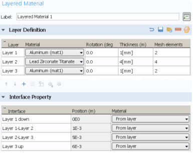
In the Model Builder window, under Global Definitions right-click Materials and choose Layered Material.
2
In the Settings window for Layered Material, locate the Layer Definition section.
3
Click  Add twice.
4
You can preview the shell cross section.
5
Click to expand the Preview Plot Settings section. In the Thickness-to-width ratio text field, type 8/30.
6
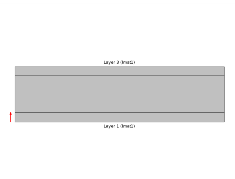
Locate the Layer Definition section. Click Layer Cross Section Preview in the upper-right corner of the section.
Add a layered material link node to make the layered material available in Component 1. Using this node, you can also select a coordinate system defining the orientation. Note that only boundary coordinate systems can be selected.
Materials
Layered Material Link 1 (llmat1)
In the Model Builder window, under Component 1 (comp1) right-click Materials and choose Layers>Layered Material Link.
Next, select only the middle layer in the shell to use the piezoelectric material.
Electric Currents in Layered Shells (ecis)
Piezoelectric Layer 1
1
In the Settings window for Piezoelectric Layer, locate the Shell Properties section.
2
Clear the Use all layers check box.
3
In the Selection table, clear the check boxes for Layer 1 and Layer 3.
Layered Shell (lshell)
Piezoelectric Material 1
1
In the Model Builder window, under Component 1 (comp1)>Layered Shell (lshell) click Piezoelectric Material 1.
2
In the Settings window for Piezoelectric Material, locate the Shell Properties section.
3
Clear the Use all layers check box.
4
In the Selection table, clear the check boxes for Layer 1 and Layer 3.
5
Locate the Piezoelectric Material Properties section. From the Constitutive relation list, choose Strain-charge form.
In the first study, the orientation of the piezoelectric layer is in the default state, that is with the pole axis normal to the base surface.
Next, set up the boundary conditions for the structure and the charge balance. Note that you need to operate with edges on the base surface.
Fixed Constraint 1
1
In the Physics toolbar, click  Edges and choose Fixed Constraint.
2
Electric Currents in Layered Shells (ecis)
Conductive Shell 1
In the Model Builder window, under Component 1 (comp1)>Electric Currents in Layered Shells (ecis) click Conductive Shell 1.
Ground 1
In the Physics toolbar, click  Boundaries and choose Ground.
Electric Potential 1
1
In the Physics toolbar, click  Boundaries and choose Electric Potential.
2
In the Settings window for Electric Potential, locate the Interface Selection section.
3
From the Apply to list, choose Bottom interface.
4
Locate the Electric Potential section. In the V0 text field, type 20.
Use a mapped mesh on the base surface of the layered shell.
Mesh 1
Mapped 1
1
In the Mesh toolbar, click  Boundary and choose Mapped.
2
In the Settings window for Mapped, locate the Boundary Selection section.
3
From the Selection list, choose All boundaries.
4
Click  Build All.
5
Click the  Go to Default View button in the Graphics toolbar.
Study 1
1
In the Model Builder window, click Study 1.
2
In the Settings window for Study, locate the Study Settings section.
3
Clear the Generate default plots check box.
4
In the Home toolbar, click  Compute.
Results
Add a special dataset that will allow a 3D representation of the layered shell extra dimension.
Layered Material 1
1
In the Model Builder window, expand the Results node.
2
Right-click Results>Datasets and choose More Datasets>Layered Material.
First, create a plot of the electric potential distribution.
Electric Potential
1
In the Results toolbar, click  3D Plot Group.
2
In the Settings window for 3D Plot Group, type Electric Potential in the Label text field.
3
Locate the Data section. From the Dataset list, choose Layered Material 1.
Surface 1
1
In the Model Builder window, right-click Electric Potential and choose Surface.
2
In the Settings window for Surface, locate the Expression section.
3
In the Expression text field, type V.
4
Locate the Coloring and Style section. From the Color table list, choose RainbowLight.
5
In the Electric Potential toolbar, click  Plot.
6
Click the  Go to Default View button in the Graphics toolbar.
Add a plot of the shell vertical displacement.
Vertical Displacement (z pole axis)
1
In the Home toolbar, click  Add Plot Group and choose 3D Plot Group.
2
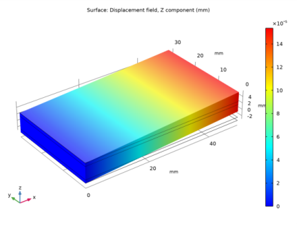
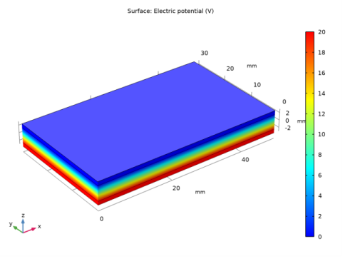
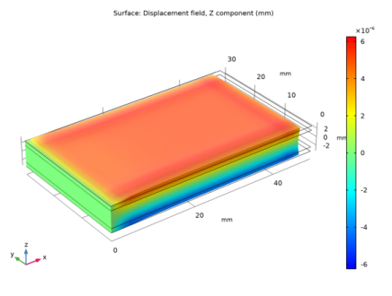
In the Settings window for 3D Plot Group, type Vertical Displacement (z pole axis) in the Label text field.
3
Locate the Data section. From the Dataset list, choose Layered Material 1.
Surface 1
1
Right-click Vertical Displacement (z pole axis) and choose Surface.
2
In the Settings window for Surface, locate the Expression section.
3
In the Expression text field, type w.
4
Locate the Coloring and Style section. From the Color table list, choose RainbowLight.
Deformation 1
1
Right-click Surface 1 and choose Deformation.
2
In the Vertical Displacement (z pole axis) toolbar, click  Plot.
3
Click the  Go to Default View button in the Graphics toolbar.
Next, change the orientation of the piezoelectric layer.
Layered Shell (lshell)
Piezoelectric Material 2
1
In the Model Builder window, under Component 1 (comp1)>Layered Shell (lshell) right-click Piezoelectric Material 1 and choose Duplicate.
2
In the Settings window for Piezoelectric Material, click to expand the Out-of-Plane Material Orientation section.
The layered material always operates with a boundary coordinate system on the base surface (laminate system). For such systems, the third base vector direction is always normal to the surface.
Use a special control if you need to change the out-of-plane orientation of the material. This is essential when the pole direction in the material data coincides with the third coordinate axis.
3
From the Use laminate coordinate system with list, choose Swapped normal and 1st tangential directions.
Add Study
1
In the Home toolbar, click  Add Study to open the Add Study window.
2
Go to the Add Study window.
3
Find the Studies subsection. In the Select Study tree, select General Studies>Stationary.
4
Click  Add Study.
5
In the Home toolbar, click  Add Study to close the Add Study window.
Add one more stationary study and recompute the results after having changed the piezoelectric material orientation.
Study 2
1
In the Settings window for Study, locate the Study Settings section.
2
Clear the Generate default plots check box.
3
In the Home toolbar, click  Compute.
Results
Layered Material 2
1
In the Model Builder window, under Results>Datasets right-click Layered Material 1 and choose Duplicate.
2
In the Settings window for Layered Material, locate the Data section.
3
From the Dataset list, choose Study 2/Solution 2 (sol2).
Finally, plot the new distribution of the vertical displacement in the structure.
Vertical Displacement (x pole axis)
1
In the Model Builder window, right-click Vertical Displacement (z pole axis) and choose Duplicate.
2
In the Settings window for 3D Plot Group, type Vertical Displacement (x pole axis) in the Label text field.
3
Locate the Data section. From the Dataset list, choose Layered Material 2.
4
In the Vertical Displacement (x pole axis) toolbar, click  Plot.
5
Click the  Go to Default View button in the Graphics toolbar.