|
|
|
|
|
|
|||
|
|
|
|||
|
|
|
|||
|
|
||||
|
|
|
|||
|
1
|
|
2
|
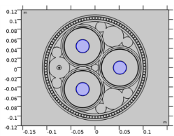
Browse to the model’s Application Libraries folder and double-click the file submarine_cable_01_introduction.mph.
|
|
3
|
|
4
|
Browse to a suitable folder and type the filename submarine_cable_04_inductive_effects.mph.
|
|
1
|
|
2
|
|
3
|
|
4
|
Browse to the model’s Application Libraries folder and double-click the file submarine_cable_c_elec_parameters.txt.
|
|
1
|
|
2
|
|
3
|
|
4
|
|
5
|
|
1
|
|
2
|
|
3
|
|
1
|
|
2
|
|
3
|
|
4
|
|
5
|
|
1
|
|
2
|
|
1
|
|
2
|
In the Model Builder window, expand the Study 1>Solver Configurations>Solution 1 (sol1)>Stationary Solver 1 node.
|
|
3
|
Right-click Study 1>Solver Configurations>Solution 1 (sol1)>Stationary Solver 1>Parametric 1 and choose Delete.
|
|
1
|
|
1
|
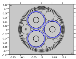
In the Model Builder window, under Component 1 (comp1) right-click Magnetic Fields (mf) and choose the domain setting Coil.
|
|
2
|
|
3
|
|
4
|
Click to collapse the Material Type section, the Coordinate System Selection section, and the Constitutive Relation sections.
|
|
5
|
|
1
|
|
2
|
|
3
|
|
4
|
|
1
|
|
2
|
|
3
|
|
4
|
|
1
|
|
2
|
|
3
|
|
4
|
|
1
|
|
2
|
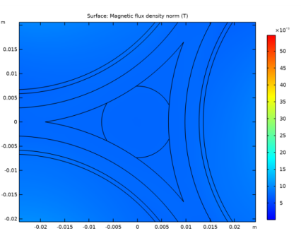
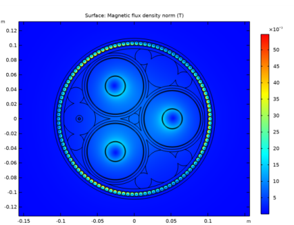
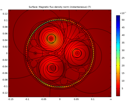
In the Settings window for 2D Plot Group, type Magnetic Flux Density Norm (mf) in the Label text field.
|
|
1
|
|
2
|
|
3
|
|
4
|
|
5
|
|
1
|
|
2
|
|
3
|
|
4
|
|
5
|
|
6
|
|
1
|
|
2
|
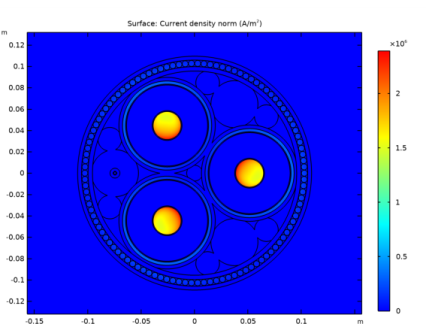
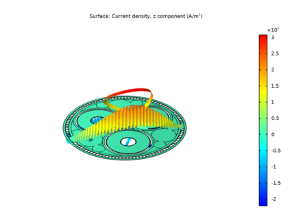
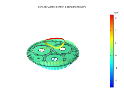
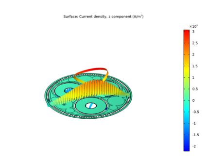
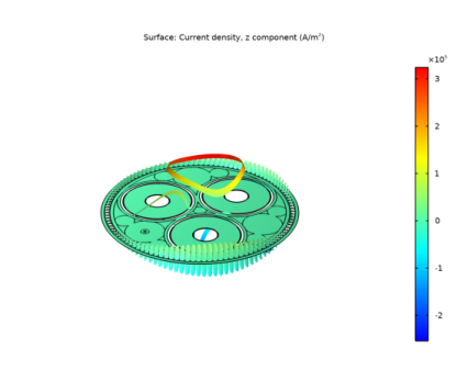
In the Settings window for 2D Plot Group, type Out of Plane Current Density (mf) in the Label text field.
|
|
3
|
|
1
|
In the Model Builder window, expand the Out of Plane Current Density (mf) node, then click Surface 1.
|
|
2
|
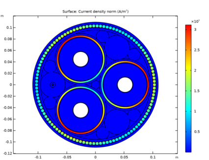
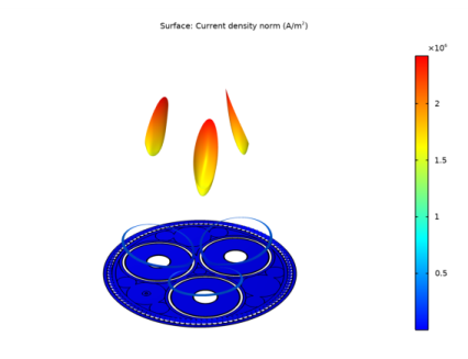
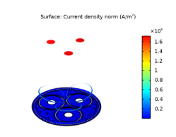
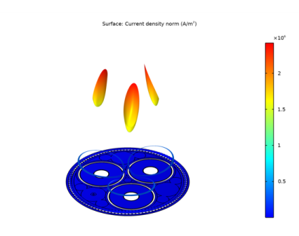
In the Settings window for Surface, click Replace Expression in the upper-right corner of the Expression section. From the menu, choose Component 1 (comp1)>Magnetic Fields>Currents and charge>mf.normJ - Current density norm - A/m², (or just type mf.normJ in the Expression field).
|
|
3
|
|
4
|
|
5
|
|
1
|
|
2
|
|
1
|
|
2
|
|
3
|
|
4
|
|
5
|
|
6
|
|
1
|
|
2
|
|
3
|
|
4
|
|
5
|
|
1
|
|
2
|
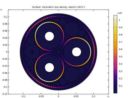
In the Settings window for 2D Plot Group, type Volumetric Loss Density (mf) in the Label text field.
|
|
1
|
|
2
|
|
3
|
|
4
|
|
5
|
|
6
|
|
1
|
|
2
|
|
3
|
|
4
|
Select the Description check box.
|
|
5
|
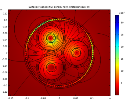
In the associated text field, type Magnetic flux density norm (instantaneous).
|
|
6
|
|
7
|
|
1
|
|
2
|
|
3
|
|
4
|
|
5
|
|
6
|
|
7
|
|
8
|
|
9
|
|
1
|
|
2
|
|
3
|
|
4
|
|
5
|
|
6
|
|
7
|
|
1
|
|
2
|
|
3
|
|
1
|
|
2
|
|
3
|
|
1
|
|
2
|
|
3
|
|
4
|
|
5
|
|
6
|
|
7
|
|
8
|
|
1
|
|
2
|
|
3
|
|
4
|
Locate the Expressions section. In the table, enter the following settings:
|
|
5
|
Click
|
|
1
|
|
2
|
|
3
|
|
4
|
Locate the Expressions section. In the table, enter the following settings:
|
|
5
|
Click
|
|
1
|
|
2
|
|
3
|
|
4
|
Locate the Expressions section. In the table, enter the following settings:
|
|
5
|
Click
|
|
1
|
Go to the Table window.
|
|
1
|
|
2
|
|
3
|
Locate the Expressions section. In the table, enter the following settings:
|
|
4
|
Click
|
|
1
|
|
2
|
|
3
|
Locate the Expressions section. In the table, enter the following settings:
|
|
4
|
Click
|
|
1
|
Go to the Table window.
|
|
1
|
|
2
|
|
3
|
|
4
|
|
5
|
|
6
|
|
1
|
|
1
|
|
2
|
|
3
|
|
1
|
|
2
|
|
1
|
|
2
|
|
3
|
In the table, update the description. Type Phase losses (2.5D model), that is; replace “plain 2D” with “2.5D”.
|
|
4
|
|
1
|
Go to the Table window.
|
|
1
|
|
2
|
|
3
|
|
4
|
|
1
|
|
2
|
|
3
|
|
4
|
|
5
|
|
1
|
|
2
|
|
3
|
|
4
|
|
5
|
|
6
|
|
1
|
|
2
|
|
3
|
|
1
|
|
2
|
|
3
|
In the table, update the description. Type Phase losses (2.5D+milliken), that is; replace “2.5D model” with “2.5D+milliken”.
|
|
4
|
|
1
|
Go to the Table window.
|
|
1
|
|
2
|
|
4
|
Click
|
|
5
|
Go to the Table window.
|
|
1
|
|
2
|
|
3
|
In the table, update the description. Type Phase inductance (2.5D+milliken), that is; replace “2.5D model” with “2.5D+milliken”.
|
|
4
|
|
5
|
Go to the Table window.
|