Tutorial Example: Modeling a Capacitive Pressure Sensor
This tutorial analyzes a hypothetical absolute pressure sensor used as an example in the book Practical MEMS, by V. Kaajakari (V. Kaajakari, Practical MEMS, Small Gear Publishing, Las Vegas, pp. 207–209, 2009). Initially the sensitivity of the device is assessed under ideal operating conditions. Then the effect of packaging induced stress is analyzed, both in terms of the device sensitivity to pressure and an induced sensitivity to temperature.
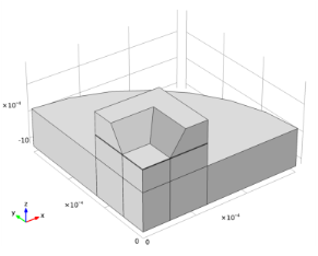
The device geometry is shown in Figure 3. The pressure sensor is part of a silicon die that has been bonded to a metal plate at 70°C. The COMSOL model takes advantage of the symmetry in the geometry and models only a single quadrant of the device.
Figure 3: The model geometry. Left: The symmetric device geometry, with the edges of one quadrant highlighted in blue, showing the symmetry planes. Right: In COMSOL only the highlighted quadrant is modeled, and the symmetry boundary condition is used on the cross section walls.
A detailed 2D section through the functional part of the device is shown in Figure 4. A thin membrane is held at a fixed potential of 1 V. The membrane is separated from a ground plane by a chamber sealed under high vacuum. The sides of the chamber are insulating to prevent a connection between the membrane and the ground plane (for simplicity the insulating layer is not modeled explicitly in the COMSOL Multiphysics model — this approximation will have little effect on the results of the study).
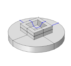
Figure 4: Cross section through the device showing the capacitor. The vertical axis has been expanded to emphasize the gap.
Pressure on the membrane from ambient gas causes the membrane to deflect. The thickness of the gap now varies across the membrane and its capacitance to ground therefore changes. This capacitance is then monitored by an interfacing circuit, such as the switched capacitor amplifier circuit discussed in the case study in Practical MEMS.
Thermal stresses are induced in the structure as a result of the thermal conductivity mismatch between the silicon die and the metal plate, and the elevated temperature used for the bonding process (assumed to be 70°C, compared to an operating temperature of 20°C). These stresses change the deformation of the diaphragm in response to applied pressures and alter the response of the sensor. In addition, since the stresses are temperature dependent, they introduce an undesired temperature dependence to the device output.
Initially the sensor is analyzed in the case where there are no packaging stresses. Then the effect of the packaging stress is considered. First, the device response at fixed temperature is evaluated with the additional packaging stress. Finally the temperature dependence of the device response at a fixed applied pressure is assessed.