PDF

Submarine Cable 5 — Bonding Inductive
Introduction
In the Inductive Effects tutorial (the previous tutorial in this series), the Coil group option is mentioned as a means to mimic the effects of cross bonding, but the exact extent of the validity of this approach is not shown. In order to investigate the different bonding types more closely, this tutorial considers three sections of cable individually, represented by three separate Magnetic Fields interfaces.
The model uses a strongly simplified geometry. Even so, the results correspond very well to those from the Inductive Effects tutorial. This justifies both the simplified geometry in this tutorial, as well as the cross-bonding approach suggested in the Inductive Effects tutorial. Finally, as opposed to the other inductive models in this series, this one allows for investigating dissimilar section lengths.
Model Definition
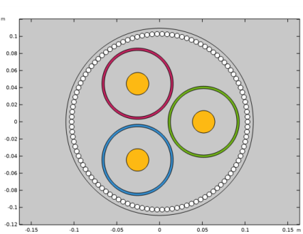
The cable geometry is heavily simplified. The geometry as used in the Capacitive, Inductive and Thermal Effects tutorials has been stripped from all details that do not significantly contribute to the inductive problem. Everything that from the inductive viewpoint can be considered an insulator has been replaced by air, leaving the three phases, the screens, and the armor; see Figure 1.
Figure 1: The simplified cable cross section, including the three phases (yellow), the screens (red, green, and blue), and the armor (white).
Theoretical Basis
When it comes to solving for the electromagnetic fields, the methods used here are identical to the ones used in the Inductive Effects tutorial. For more details on the involved electromagnetic theory, see that tutorial’s theory section.
As for the Electrical Circuit interface, this is governed by Kirchhoff’s circuit laws. Based on the principles of conservation of electric charge and conservation of energy, they state the following:
1
2
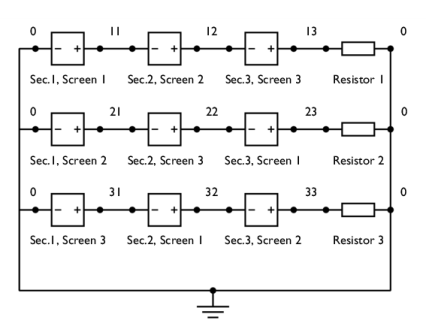
In addition to this, there is the two-way coupling between the circuit and the three finite element models: The current that is dictated by the circuit is applied in the Magnetic Fields interfaces. Here, by integrating the electric field, the electromotive force (emf) is determined. The resulting voltage is fed back into the circuit as a potential difference. For each series chain (see Figure 2), the sum of the potential differences from the three screens gives the potential across a small helper resistor1, which responds with a current. This current is then fed back into the finite element models, making the two-way coupling complete.
Modeling Approach
The tutorial starts with the basics, by exciting a current in the phases using a Coil feature with the setting Single conductor applied2. The currents induced by the electromotive force (emf) in the screens may flow freely; there is no restriction in the out-of-plane direction. This configuration is effectively the same as Solid Bonding.
In a second step, three additional Coil features are added. These set the total net cross-sectional current to zero for each screen individually, while still allowing for variations within the screens. This configuration is effectively the same as Single-Point Bonding.
In a third step, two duplicate Magnetic Fields interfaces are created, resulting in one separate finite element model for each cable section. Al three Magnetic Fields interfaces are then set to an out-of-plane thickness of one third of the total cable length.
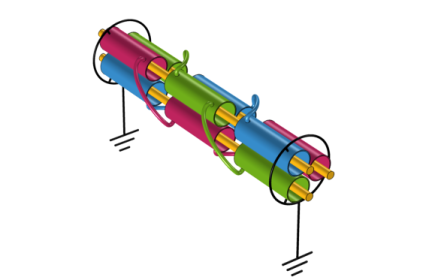
The six screens that result are connected to a circuit, as given by Figure 2. A two-way coupling is achieved by using a Coil domain in the Magnetic Fields interface, and an External I Vs. U feature in the Electrical Circuits interface. The resulting configuration is effectively identical to Cross Bonding.
The results are compared to those found in the Inductive Effects tutorial. Finally, you will be encouraged to try dissimilar section lengths, as this is something the other inductive models in this series cannot do.
Figure 2: The cross bonding scheme, as it appears in the electrical circuit, including positive/negative indication, node numbers, and screen- and section numbers.
On Bonding Types
Solid Bonding
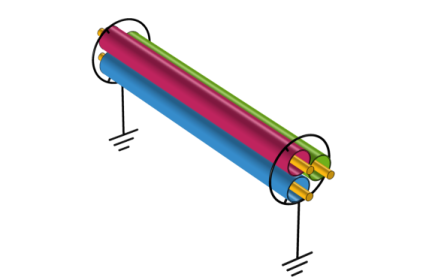
In case of solid bonding, each screen is electrically paired with the same phase across the entire length of the cable. Furthermore, it is bonded and connected to ground at both ends; see Figure 3.
For the inductive problem, this means circulating currents will flow. As the three phase currents have a 120° phase difference, so will the currents induced by their electromotive force (emf) in the screens: The currents pushed forward by screen 1, will enter the bonding points and then flow back through screen 2 and screen 3. In a well balanced cable the sum of the currents from all three screens will be zero, so there will be no net current flowing from one ground point to the other.
Notice that from the inductive viewpoint, in this configuration it does not make sense to talk about an electric scalar potential V (not in the stationary-electric sense anyway). Screen currents will flow back and forth, yet on both ends of the cable the electric potential is 0 V (as the screen is connected to ground). The traditional stationary-electric reasoning fails here, because the electric fields are not curl-free3. The electric potential that does occur in the screens, is caused by the charging currents, as treated in the Bonding Capacitive tutorial.
Figure 3: Schematic depiction of solid bonding, where the screens (red, green, and blue) are bonded and grounded at both ends.
This configuration may be the least efficient of the tree bonding types — the screen losses are high, as seen in the Inductive Effects tutorial — but it is also the most robust one. Since submarine cables are supposed to have a life expectancy of about forty years (with repairs being very costly), this is the preferred choice. Single-point bonding would increase the chances of having corrosion phenomena at one end of the cable, and cross bonding would complicate matters even further.
Single-Point Bonding
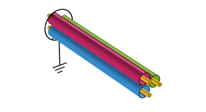
In case of single-point bonding, each screen is still paired with a single phase, but this time it is bonded and connected to ground at one end only; see Figure 4. The magnetic fields from the phase currents will still induce an emf across the screens, but since there is no closed circuit, circulating currents will not form. In this case, it does make sense to talk about a magnetically induced electric potential in the screens: The voltage at the floating end is induced by both capacitive and inductive phenomena.
Figure 4: Schematic depiction of single-point bonding, where the screens (red, green, and blue) are bonded and grounded at one end only.
And it is this voltage that limits the applicability of this configuration. The cable system must be designed to limit the screen voltage to a locally permitted level (around 3 to 5 kV). Special care needs to be taken to prevent excessive voltage built up due to transient effects or screen-to-earth faults. For the end that is not bonded, surge voltage limiters or arc suppression coils are applied (ARC, also known as a Petersen coil).
The induced voltages in the screens are directly proportional to both the currents in the phases — or, more precisely, their time derivative — as well as the total length of the cable. Consequently, this configuration is used for shorter stretches only. Because of the increased risk of corrosion, it is mainly used for terrestrial applications (as opposed to submarine)4.
Cross Bonding
Cross bonding shows the most sophisticated configuration — and conceptually, the most elegant one. In case of cross bonding, the total length of cable is split in three sections of equal length. From an electrical point of view, the screen is paired with a different phase for each section; see Figure 5.
As for each electrically connected set of screens the electromotive forces in the three cable sections show a 120° phase shift, the effects cancel out: For a well balanced cable, the total net current induced in the screens will be zero5.
Figure 5: Schematic depiction of cross bonding, where the screens (red, green, and blue) are split in three cross-bonded sections of equal length.
In this configuration, the maximum screen voltage occurs at the intersections. Like for single-point bonding, precautions need to be taken to limit the screen voltage to a certain level. The intersections increase the complexity of the cable system, and consequently, the risk of failure (due to leakage, corrosion and such). Therefore, like for single-point bonding, this configuration is not preferred for submarine cable systems6.
Results and Discussion
The first tested bonding configuration (solid bonding), is more or less a direct copy of the plain 2D model discussed in the Inductive Effects tutorial. And indeed, the results are practically identical, even though the geometry is strongly simplified: The screen and phase losses are about 13 kW/km and 47 kW/km, still.
When switching to single-point bonding, the screen losses go down significantly, to 2.9 kW/km. As a direct consequence, the AC resistance goes down too, to 45 mΩ/km (approaching the DC one, as expected). A redistribution of magnetic energy leads to some watered effects7, raising the phase losses marginally. The absolute voltage induced across the screens is about 473 V.
Finally, when using cross bonding, all results remain the same except for the screen voltages. Across each section, there is a 158 V potential difference. As the voltages across the three consecutive screens in a series chain (Figure 2) show a 120° phase shift, the screen potential along the cable8 will form an equilateral triangle on the complex plane (with one tip connected to ground).
On Accuracy
The first tested configuration shows an almost perfect agreement with the much more detailed plain 2D model from the Inductive Effects tutorial. This is, of course, a very nice result as it legitimates this model as a means to investigate the different bonding types for the more detailed versions.
When you start to think about it however, the results agree so well, it is a bit confronting: It basically means that — at least from an inductive viewpoint — all the nice little details that we have been adding to the geometry so far, have been inconsequential (that includes the detailed mesh and the additional computational effort).
Most of the material properties that we have been entering so carefully in the Introduction tutorial, have been inconsequential as well. This is similar to the observation done in the Capacitive Effects tutorial, where the cable’s capacitive properties are found to be given by a fairly simple analytical expression containing one material property only.
The observation that these details are inconsequential, however, does not make them meaningless. Proving something to be insignificant by adding it to a numerical model is a perfectly viable strategy. It is a good way to investigate what is important about a device.
A common misconception is to think a more detailed model is by definition a more accurate one. As these results show, it is not the amount of details that makes a good model; it is the kind of details.
Application Library path: ACDC_Module/Tutorials,_Cables/submarine_cable_05_bonding_inductive
Modeling Instructions
From the File menu, choose New.
New
In the New window, click  Model Wizard.
Model Wizard
1
In the Model Wizard window, click  2D.
2
In the Select Physics tree, select AC/DC>Electromagnetic Fields>Magnetic Fields (mf).
3
Click Add.
4
Click  Study.
5
In the Select Study tree, select General Studies>Frequency Domain.
6
Global Definitions
This model uses a subset of the parameters already defined for the other tutorials. In order to gain access to them, you can load them all. While doing so, you can adjust the cable length parameters to match the first bonding type investigated (solid bonding).
Geometric Parameters 1
1
In the Model Builder window, under Global Definitions click Parameters 1.
2
In the Settings window for Parameters, type Geometric Parameters 1 in the Label text field.
3
Locate the Parameters section. Click  Load from File.
4
Geometric Parameters 2
1
In the Home toolbar, click  Parameters and choose Add>Parameters.
2
In the Settings window for Parameters, type Geometric Parameters 2 in the Label text field.
3
Locate the Parameters section. Click  Load from File.
4
5
In the table, adjust the parameters Lsec1 and Lsec3 as follows:
Electromagnetic Parameters
1
In the Home toolbar, click  Parameters and choose Add>Parameters.
2
In the Settings window for Parameters, type Electromagnetic Parameters in the Label text field.
3
Locate the Parameters section. Click  Load from File.
4
Geometry 1
As this tutorial intents to focus on the effects of bonding types, the geometry is kept simple. From the Inductive Effects tutorial we know the fiber may be neglected. Furthermore, the insulators have little or no influence on the inductive part and may just as well be replaced by air. What we are left with is a number of circles representing the copper, the lead and the steel.
Start by adding one phase, together with its screen. By setting their labels, and enabling the Resulting objects selection, you automatically set a domain selection that coincides with the shape you create. The selections will then propagate through the sequence (when a shape is copied, its selection will cover both the original and the copy).
Phases
1
In the Geometry toolbar, click  Circle.
2
In the Settings window for Circle, type Phases in the Label text field.
3
Locate the Size and Shape section. In the Radius text field, type Dcon/2.
4
Locate the Position section. In the x text field, type Dpha/sqrt(3).
5
Locate the Selections of Resulting Entities section. Select the Resulting objects selection check box.
6
Click  Build Selected.
7
Click the  Zoom Extents button in the Graphics toolbar.
Screens
1
Right-click Phases and choose Duplicate.
2
In the Settings window for Circle, type Screens in the Label text field.
3
Locate the Object Type section. From the Type list, choose Curve.
4
Locate the Size and Shape section. In the Radius text field, type Dins/2+Tpbs.
5
Click to expand the Layers section. In the table, enter the following settings:
6
Click  Build Selected.
7
Click the  Zoom Extents button in the Graphics toolbar.
Next, create rotated copies of the phase and screen. Unify the objects in order to remove unnecessary interior boundaries.
Rotate 1 (rot1)
1
In the Geometry toolbar, click  Transforms and choose Rotate.
2
Click in the Graphics window and then press Ctrl+A to select both objects.
3
In the Settings window for Rotate, locate the Rotation section.
4
In the Angle text field, type 0[deg], 120[deg], 240[deg].
5
Click  Build Selected.
6
Click the  Zoom Extents button in the Graphics toolbar.
Union 1 (uni1)
1
In the Geometry toolbar, click  Booleans and Partitions and choose Union.
2
Click in the Graphics window and then press Ctrl+A to select all objects.
3
In the Settings window for Union, locate the Union section.
4
Clear the Keep interior boundaries check box.
5
Click  Build Selected.
Note this is just one of many different ways to get to this result. The rings for example, could alternatively have been made by adding circles of radius Dins/2+Tpbs, and subtracting from those, circles of radius Dins/2 (again, using Booleans and Partitions).
For the armor, there should be an integer amount of wires in the cable’s circumference. This number, Narm, is stored as a parameter. Use the Rotate transform and the range() operator, to distribute the wires equally in the interval [0,360] degrees.
Cable Armor
1
In the Geometry toolbar, click  Circle.
2
In the Settings window for Circle, type Cable Armor in the Label text field.
3
Locate the Size and Shape section. In the Radius text field, type Tarm/2.
4
Locate the Position section. In the x text field, type Darm/2.
5
Locate the Selections of Resulting Entities section. Select the Resulting objects selection check box.
6
Click  Build Selected.
Rotate 2 (rot2)
1
In the Geometry toolbar, click  Transforms and choose Rotate.
2
In the Settings window for Rotate, locate the Input section.
3
From the Input objects list, choose Cable Armor.
4
In the Settings window for Rotate, locate the Rotation section.
5
In the Angle text field, type 360[deg]*range(1/Narm,1/Narm,1).
6
Click  Build Selected.
Finally, add some circles indicating the cable-soil interface and the outer boundary of the modeling domain.
Cable Domains
1
In the Geometry toolbar, click  Circle.
2
In the Settings window for Circle, type Cable Domains in the Label text field.
3
Locate the Size and Shape section. In the Radius text field, type Dcab/2.
4
Locate the Selections of Resulting Entities section. Select the Resulting objects selection check box.
5
Click  Build Selected.
6
Click the  Zoom Extents button in the Graphics toolbar.
Electromagnetic Domains
1
Right-click Cable Domains and choose Duplicate.
2
In the Settings window for Circle, type Electromagnetic Domains in the Label text field.
3
Locate the Size and Shape section. In the Radius text field, type 5*Dcab/2.
Form Union (fin)
1
In the Geometry toolbar, click  Build All.
2
Click the  Zoom Extents button in the Graphics toolbar.
Definitions
The materials are roughly the same as those used in the Inductive Effects tutorial. To start with, you can modify the View to show the material colors. Then, the materials will be added, they will be given an appropriate label (if they do not already have it), a selection and an appearance.
View 1
1
In the Model Builder window, expand the Component 1 (comp1)>Definitions node, then click View 1.
2
In the Settings window for View, locate the Colors section.
3
Select the Show material color and texture check box.
Add Material
1
In the Home toolbar, click  Add Material to open the Add Material window.
2
Go to the Add Material window.
3
4
Click  Add to Component 1 (comp1).
5
In the Home toolbar, click  Add Material to close the Add Material window.
Materials
Air (mat1)
1
Click the  Zoom to Selection button in the Graphics toolbar.
A good approach is to assign the first material to all domains by default. Subsequently, you can override it locally, using additional materials. This ensures every domain has access to material properties.
Copper
1
In the Model Builder window, right-click Materials and choose Blank Material.
2
In the Settings window for Material, type Copper in the Label text field.
3
Locate the Geometric Entity Selection section. From the Selection list, choose Phases.
4
Click the Zoom In button in the Graphics toolbar, twice.
5
Click to expand the Appearance section. From the Family list, choose Copper.
Lead
1
Right-click Materials and choose Blank Material.
2
In the Settings window for Material, type Lead in the Label text field.
3
Locate the Geometric Entity Selection section. From the Selection list, choose Screens.
4
Click to expand the Appearance section. From the Family list, choose Lead.
Galvanized steel
1
Right-click Materials and choose Blank Material.
2
In the Settings window for Material, type Galvanized steel in the Label text field.
3
Locate the Geometric Entity Selection section. From the Selection list, choose Cable Armor.
4
Click to expand the Appearance section. From the Family list, choose Steel.
Materials
Now, you will see that COMSOL starts detecting missing material properties. The properties that should be added are listed in the following table. Please check all of them for the correct value, even the ones that are already filled in. Note that for cases like this, a convenient option is to copy-paste the values directly from this *.pdf file to COMSOL.
1
In the Model Builder window, under Component 1 (comp1)>Materials, add the following material properties:
Modeling Instructions — Solid Bonding
In case of solid bonding, each screen is electrically paired with the same phase across the entire length of the cable. Furthermore, it is bonded and grounded at both ends. The electromotive force (emf) from the main conductors will induce a current in the screens, see section Solid Bonding.
Let us reproduce this behavior. Start by setting the interface label, and the out-of-plane thickness. Then, introduce the coil domains needed for setting the phase currents.
Magnetic Fields, Section 1
1
In the Model Builder window, under Component 1 (comp1) click Magnetic Fields (mf).
2
In the Settings window for Magnetic Fields, type Magnetic Fields, Section 1 in the Label text field.
3
Locate the Thickness section. In the d text field, type Lsec1*Lcab.
Phase 1
1
In the Physics toolbar, click  Domains and choose Coil.
2
In the Settings window for Coil, type Phase 1 in the Label text field.
3
The settings window for the coil feature contains a lot of sections. For many of these, the default settings are sufficient. Collapse them to have a closer look at the important part; the Coil section.
4
Click to collapse the Material Type section, the Coordinate System Selection section, and the Constitutive Relation sections.
Next, proceed by setting the currents.
5
Locate the Coil section. In the Icoil text field, type I0.
Phase 2
1
In the Physics toolbar, click  Domains and choose Coil.
2
In the Settings window for Coil, type Phase 2 in the Label text field.
3
4
Locate the Coil section. In the Icoil text field, type I0*exp(-120[deg]*j).
Phase 3
1
In the Physics toolbar, click  Domains and choose Coil.
2
In the Settings window for Coil, type Phase 3 in the Label text field.
3
4
Locate the Coil section. In the Icoil text field, type I0*exp(+120[deg]*j).
For more details on the coil settings, please have a look at the Inductive Effects tutorial. Proceed by computing the result.
Study 1
Step 1: Frequency Domain
1
In the Model Builder window, under Study 1 click Step 1: Frequency Domain.
2
In the Settings window for Frequency Domain, locate the Study Settings section.
3
In the Frequencies text field, type f0.
4
In the Home toolbar, click  Compute.
Results
Magnetic Flux Density Norm (mf)
In the Magnetic Flux Density Norm (mf) toolbar, click  Plot.
Assuming you have been through the previous tutorial in this series, the default Magnetic Flux Density Norm plot should look fairly familiar. We will not adjust it this time (the topic has been treated in detail in the Inductive Effects tutorial). Instead, let us have a look at the corresponding losses.
Phase Losses
1
In the Results toolbar, click  More Derived Values and choose Integration>Surface Integration.
2
In the Settings window for Surface Integration, type Phase Losses in the Label text field.
3
Locate the Selection section. From the Selection list, choose Phases.
4
Locate the Expressions section. In the table, enter the following settings:
5
Click  Evaluate.
Screen Losses
1
In the Results toolbar, click  More Derived Values and choose Integration>Surface Integration.
2
In the Settings window for Surface Integration, type Screen Losses in the Label text field.
3
Locate the Selection section. From the Selection list, choose Screens.
4
Locate the Expressions section. In the table, enter the following settings:
5
Click  Evaluate.
Table
1
Go to the Table window.
The losses per kilometer should be about 47 kW and 13 kW for the phases and screens respectively.
The resemblance with the results from the Inductive Effects tutorial are striking, confronting even. It is a clear sign that many details included in the initial model have been superfluous in the end (for a reflection on this, see section On Accuracy).
At the same time, these results show this is a valid simplification. Feel free to verify these statements. Please be cautious however, when comparing this model to the one from the Inductive Effects tutorial; be aware of the difference between the plain 2D model, the 2.5D model, and the one with the milliken conductors.
Let us see if the same goes for the lumped parameters:
Results
Phase AC Resistance
1
In the Results toolbar, click  Global Evaluation.
2
In the Settings window for Global Evaluation, type Phase AC Resistance in the Label text field.
3
Locate the Expressions section. In the table, enter the following settings:
4
Click  Evaluate.
Phase Inductance
1
In the Results toolbar, click  Global Evaluation.
2
In the Settings window for Global Evaluation, type Phase Inductance in the Label text field.
3
Locate the Expressions section. In the table, enter the following settings:
4
Click  Evaluate.
Table
1
Go to the Table window.
Here too, the resemblance is striking (53 mΩ/km and 0.42 mH/km). Furthermore, notice these results are symmetric while the detailed plain 2D model in the Inductive Effects tutorial shows a slight but consistent difference between the phases. This effect is caused by the fiber’s armor.
As the currents in the screens can flow freely, the losses are comparably high. This leads to a high phase AC resistance. One way to bring down the screen losses, is by means of single-point bonding.
Modeling Instructions — Single-Point Bonding
In case of single-point bonding, each screen is still paired with a single phase, but this time it is bonded and grounded at one end only. The phase currents will still generate an electromotive force (emf) in the screens, but since there is no closed circuit, no net current will flow (see section Single-Point Bonding).
Let us reproduce this behavior. Introduce the coil domains needed to suppress the screen currents.
Magnetic Fields, Section 1 (mf)
Screen 1
1
In the Physics toolbar, click  Domains and choose Coil.
2
In the Settings window for Coil, type Screen 1 in the Label text field.
3
4
Locate the Coil section. In the Icoil text field, type 0[A].
Screen 2
1
In the Physics toolbar, click  Domains and choose Coil.
2
In the Settings window for Coil, type Screen 2 in the Label text field.
3
4
Locate the Coil section. In the Icoil text field, type 0[A].
Screen 3
1
In the Physics toolbar, click  Domains and choose Coil.
2
In the Settings window for Coil, type Screen 3 in the Label text field.
3
4
Locate the Coil section. In the Icoil text field, type 0[A].
Here, you have used the Coil feature to set a zero net current for each screen individually. When solving the model, an out-of-plane voltage will be applied such that the total current per screen is 0[A]. This voltage will be equal in magnitude to the one induced by the electromotive force, but opposite in sign. Proceed by computing the results.
Study 1
In the Home toolbar, click  Compute.
Feel free to re-evaluate Derived Values>Phase Losses, Screen Losses, Phase AC Resistance, and Phase Inductance.
When doing so, please do not forget to update the descriptions in the expression tables — change “Phase losses (solid bonding)” to “Phase losses (single-point bonding)”, and so on... Otherwise, distinguishing the results for the various bonding types may be difficult.
Table
1
Go to the Table window.
The phase losses and the inductance should go up slightly (to 47 kW/km and 0.43 mH/km), the screen losses should go down significantly (to 2.9 kW/km), and the phase AC resistance should go down as well, to 45 mΩ/km, approaching the DC value given by Rcon; 34 mΩ/km.
Now, let us check the voltages induced in the screens, across the length of the cable.
Results
Screen Voltage
1
In the Results toolbar, click  Global Evaluation.
2
In the Settings window for Global Evaluation, type Screen Voltage in the Label text field.
3
Locate the Expressions section. In the table, enter the following settings:
4
Click  Evaluate.
Table
1
Go to the Table window.
So the voltage in the screen at the end that is floating, will oscillate with an amplitude of about 473 V. Note that if you remove the abs(...) operator from the expression, you will get three different complex values for screen 1, 2, and 3, each of them having a phase shift of 120° with respect to the other two.
The longer the cable and the stronger the phase current, the higher the induced voltage. As a consequence, single-point bonding is only suitable for limited lengths of cable. Cross bonding is suitable for much longer stretches.
Modeling Instructions — Cross Bonding
In case of cross bonding, the total length of cable is split in three sections of equal length. From an electrical point of view, the screen is paired with a different phase for each section. Consequently, for a well balanced cable, the total net current induced in the screens will be zero (see section Cross Bonding).
In the Inductive Effects tutorial, we suggested modeling cross bonding by putting the three screens in series directly, using a Coil group. We will not do that here for two reasons: First of all, one of the main goals of this model is to verify this method, so we need to come up with something that is closer to the actual situation. Secondly, in doing so, we create a model that not only supports three sections of equal length, but sections of arbitrary length.
When verifying, we need sections of equal length though. Start by updating the parameters.
Global Definitions
Geometric Parameters 2
1
In the Model Builder window, under Global Definitions click Geometric Parameters 2.
2
In the Settings window for Parameters, locate the Parameters section.
3
In the table, modify the parameters Lsec1 and Lsec3 as follows:
Introduce two new Magnetic Fields interfaces (in order to end up with one for each section). Add an Electrical Circuit interface to connect the screens according to the cross bonding scheme, as shown in Figure 2.
Add Physics
1
In the Home toolbar, click  Add Physics to open the Add Physics window.
2
Go to the Add Physics window.
3
In the tree, select AC/DC>Electromagnetic Fields>Magnetic Fields (mf).
4
Click Add to Component 1 in the window toolbar.
5
In the tree, select AC/DC>Electromagnetic Fields>Magnetic Fields (mf).
6
Click Add to Component 1 in the window toolbar.
7
In the tree, select AC/DC>Electrical Circuit (cir).
8
Click Add to Component 1 in the window toolbar.
9
In the Home toolbar, click  Add Physics to close the Add Physics window.
Magnetic Fields, Section 2
1
In the Model Builder window, under Component 1 (comp1) click Magnetic Fields 2 (mf2).
2
In the Settings window for Magnetic Fields, type Magnetic Fields, Section 2 in the Label text field.
3
Locate the Thickness section. In the d text field, type Lsec2*Lcab.
Magnetic Fields, Section 3
1
In the Model Builder window, under Component 1 (comp1) click Magnetic Fields 3 (mf3).
2
In the Settings window for Magnetic Fields, type Magnetic Fields, Section 3 in the Label text field.
3
Locate the Thickness section. In the d text field, type Lsec3*Lcab.
Now that you have introduced one Magnetic Fields interface for each section, you can copy-paste the Coil features from one section to the other. Start by setting the correct excitation form.
Magnetic Fields, Section 1 (mf)
Screen 1
1
In the Model Builder window, under Component 1 (comp1)>Magnetic Fields, Section 1 (mf) click Screen 1.
2
In the Settings window for Coil, locate the Coil section.
3
From the Coil excitation list, choose Circuit (current).
Screen 2, Screen 3
Repeat these steps for Screen 2, and Screen 3.
Phase 1, Phase 2, Phase 3, Screen 1, Screen 2, Screen 3
1
In the Model Builder window, under Component 1 (comp1)>Magnetic Fields, Section 1 (mf), Ctrl-click to select Phase 1, Phase 2, Phase 3, Screen 1, Screen 2, and Screen 3.
(Apply a multinode selection; 6 nodes in total).
2
Magnetic Fields, Section 2 (mf2), Section 3 (mf3)
1
In the Model Builder window, under Component 1 (comp1) right-click Magnetic Fields, Section 2 (mf2) and choose Paste Multiple Items.
2
Repeat these steps for Magnetic Fields, Section 3 (mf3).
Electrical Circuit (cir)
The screens will be connected as depicted in Figure 2. You can build the circuit using this figure as a reference (please browse through the next pages before starting however, as they contain additional advice). The detailed modeling instructions for the first series chain are as follows:
In the Model Builder window, under Component 1 (comp1) click Electrical Circuit (cir).
External I vs. U 1
1
In the Electrical Circuit toolbar, click  External I vs. U.
2
In the Settings window for External I vs. U, locate the Node Connections section.
3
4
Locate the External Device section. From the V list, choose Coil voltage (mf/coil4).
External I vs. U 2
1
In the Electrical Circuit toolbar, click  External I vs. U.
2
In the Settings window for External I vs. U, locate the Node Connections section.
3
4
Locate the External Device section. From the V list, choose Coil voltage (mf2/coil5).
External I vs. U 3
1
In the Electrical Circuit toolbar, click  External I vs. U.
2
In the Settings window for External I vs. U, locate the Node Connections section.
3
4
Locate the External Device section. From the V list, choose Coil voltage (mf3/coil6).
Resistor R1
1
In the Electrical Circuit toolbar, click  Resistor.
2
In the Settings window for Resistor, locate the Node Connections section.
3
4
Locate the Device Parameters section. In the R text field, type 1[uohm].
This connects the first screen from Section 1, the second screen from Section 2, and the third screen from Section 3, in series.
External I Vs. U 4,5,6,7,8,9, Resistor R2,3
1
2
Although their value is small, the resistors serve a crucial purpose. The External I Vs. U feature feeds a current from the circuit into the Coil feature. The coil feature responds with an induced voltage. This voltage in turn, is fed back into the circuit.
From the circuit’s viewpoint, the External I Vs. U features behave like ideal voltage sources without any internal resistance. In order to complete the two-way physics coupling, the circuit needs to be able to accept these voltages and respond with a current. For this, it will need some internal resistance (see section Theoretical Basis).
Now that the circuit is complete, it is time to collect the results. Let us compute.
Study 1
1
In the Home toolbar, click  Compute.
Hint; if you get errors like “The DAE is structurally inconsistent”, it probably means you have a loose connection. In that case, please check your node numbers (p and n).
Table
1
Go to the Table window.
Feel free to re-evaluate Derived Values>Phase Losses, Screen Losses, Phase AC Resistance, and Phase Inductance. Do not forget to update the descriptions in the tables — change “Phase losses (single-point bonding)” to “Phase losses (cross bonding)”, and so on... The resulting figures should be the same as last time and they should be the same for Magnetic Fields 1,2,3. The voltages however, are different now.
Results
Screen Voltage
1
In the Model Builder window, under Results>Derived Values click Screen Voltage.
2
In the Settings window for Global Evaluation, locate the Expressions section.
3
In the table, update the descriptions. Type Voltage across screen 1,2,3 (cross bonding), that is; replace “single-point bonding” with “cross bonding”.
4
In the Settings window for Global Evaluation, click  Evaluate.
Table
1
Go to the Table window.
The absolute voltage across each screen in one section of the cable, is about 158 V. Since for each series chain the voltage across each section shows a 120° phase shift with respect to the other two, the total voltage drop along the chain will be zero. Apart from some charge current (see the Bonding Capacitive tutorial), the total net current in the screens will therefore be zero.
The resulting losses and lumped parameters are the same as those in the Inductive Effects tutorial, when putting the screens in series by means of a Coil group (thus, validating that approach). You will see the results remain consistent, even if you de-balance the cable.
There is one thing the Inductive Effects model can not do however: Testing dissimilar section lengths. Please feel free to change Lsec1 and Lsec3. Be careful not putting them to zero though, as that would change the number of sections. Furthermore, be careful not to misinterpret lumped quantities for de-balanced cables. For de-balanced cables, a variable like mf.RCoil_1 merely reflects (the real part of) the ratio between the voltage over a phase and the current through that phase. It does not tell you to what degree those voltages and currents (and losses) are caused by the phase itself, or its neighbors.
You have now completed this tutorial, subsequent tutorials will refer to the resulting file as submarine_cable_05_bonding_inductive.mph. The next tutorial in this series will include a detailed thermal analysis.
1
From the File menu, choose Save As.
2
Browse to a suitable folder and type the file name submarine_cable_05_bonding_inductive.mph.
 

1
Note that the resistor needs to be properly scaled with respect to the screen’s internal resistance. If the resistor is too small, the model will become ill-posed (similar to the issue we encountered in the Capacitive Effects tutorial), if the resistor is too large, it will significantly influence the results by suppressing the screen currents. As a rule of thumb, a value of about 10-6 times the screen resistance is advised.

2
For more information on the coil feature and its settings, see the Inductive Effects tutorial in this series.

3
If this phenomenon seems strange to you, please consider the classical textbook example of a metal ring in a time-harmonic magnetic field: It has no beginning or end (no + or - terminal), there is no battery or ground point, yet a current is flowing — forward on one side, back on the other.

4
Treatment of the single-point bonding configuration within the context of this submarine cable tutorial series should therefore be seen as a demonstration of a concept, rather than a demonstration of a real-world application. Including these bonding types extends this tutorial series to a point where it is useful for demonstrating terrestrial applications as well.

5
Note that this does not hold entirely for the charging currents; see the Bonding Capacitive tutorial.

6
Treatment of the cross bonding configuration within the context of this submarine cable tutorial series should therefore be seen as a demonstration of a concept, rather than a demonstration of a real-world application.

7
For more on this, see the Inductive Effects tutorial — in particular the parts where the armor twist and the phase twist are introduced.

8
The screen potential due to inductive effects, that is. The raise in screen potential due to capacitive effects is discussed in the Capacitive Effects tutorial.