PDF

Planar PCB Coil
Introduction
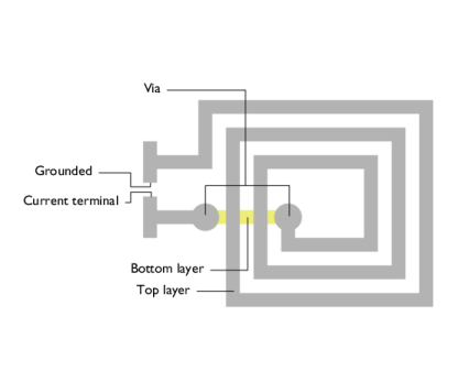
Planar coils on printed-circuit board (PCB) are widely used for instance in radio-frequency identification, wireless charging and micro-motor devices. This tutorial example shows how to use the Electric Currents in Shells physics interface together with the Magnetic Field physics interface to compute the resistance and inductance of a planar PCB coil. The Electric Currents in Shells interface offers the advantage of drawing the entire coil layout as flat and on the same plane. A coil with three turns and two vias as represented in Figure 1 is modeled but the model showcases functionality that is applicable to a wide range of geometric configurations.
Figure 1: The structure of a simple PCB coil.
Model Definition
The planar PCB coil is made of copper of 0.1 mm thickness. The current flows from one terminal on the top layer to the bottom layer through a via, back to the top layer through a second via and then to the other terminal that is grounded. It is worth noticing that the use of selections has made it possible to automatically identify all the crossings. The PCB substrate is typically made of epoxy resin, providing insulation between conducting layers. Since only the current conduction is of interest, the model uses air material settings (zero conductivity) also in the substrate.
Solving the electric currents, shell problem yields the electric potential drop along the conductor, and the lumped resistance R is computed according to Ohm’s law
(1)
where U is the electric potential at the current terminal and I is the injected current (1 A in the current model setup). The computed surface current density flowing in the coil is then applied as the source term in the Amperè’s law to compute the magnetic field distribution in the space surrounding the coil.
Note that here the electric currents have been computed for an open path. However, when dealing with magnetic fields, closing the current path is compulsory as current/charge conservation is inherent in Amperè’s law. For this purpose, an extra magnetic insulation surface is added between the ground and current terminal. It will carry a reaction (numerically induced) surface current density, making the solution self-consistent with the divergence free nature of currents in Amperè’s law.
The inductance can be derived as the ratio of linked magnetic flux to current. For the case of a single coil, the inductance can also be calculated using current and magnetic energy. In particular coil inductance can be expresses as
(2)
where Wm is the total magnetic energy in the space.
Results and Discussion
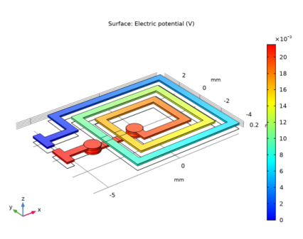
The model is solved using the default stationary solver. The plot for the electric potential distribution on the surface of the coil is shown in Figure 2. Note that this default plot automatically places the layers in their appropriate positions.
Figure 2: Electric potential distribution on the surface of the PCB coil.
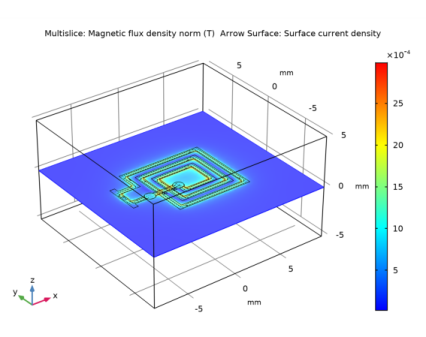
The default magnetic field plot is shown in Figure 3. Arrows displaying the surface current density on the coil have been added.
Figure 3: The simulated surface current density of the coil and the magnetic field around it.
As a final step, the coil resistance and inductance are evaluated to 21.5 mΩ and 0.06 μH respectively.
Application Library path: ACDC_Module/Layered_Shell/planar_pcb_coil
Modeling Instructions
From the File menu, choose New.
New
In the New window, click Model Wizard.
Model Wizard
1
In the Model Wizard window, click 3D.
2
In the Select Physics tree, select AC/DC>Electric Fields and Currents>Electric Currents in Shells (ecis).
3
Click Add.
4
Click Study.
5
In the Select Study tree, select General Studies>Stationary.
6
Click Done.
Global Definitions
In the Home toolbar, click Windows and choose Add Material from Library.
Add Material
1
Go to the Add Material window.
2
In the tree, select Built-in>Copper.
3
Click Add to Global Materials in the window toolbar.
Global Definitions
In the Home toolbar, click Windows and choose Add Material from Library.
Add Material
1
Go to the Add Material window.
2
In the tree, select Built-in>FR4 (Circuit Board).
3
Click Add to Global Materials.
Global Definitions
Layered Material 1 (lmat1)
1
In the Model Builder window, under Global Definitions right-click Materials and choose Layered Material.
2
In the Settings window for Layered Material, type Upper metalization in the Label text field.
3
Locate the Layer Definition section. In the table, enter the following settings:
Layered Material 2 (lmat2)
1
Right-click Materials and choose Layered Material.
2
In the Settings window for Layered Material, type Lower metallizzaton in the Label text field.
3
Locate the Layer Definition section. In the table, enter the following settings:
Layered Material 3 (lmat3)
1
Right-click Materials and choose Layered Material.
2
In the Settings window for Layered Material, type Vias metallization in the Label text field.
3
Locate the Layer Definition section. In the table, enter the following settings:
Geometry 1
1
In the Model Builder window, under Component 1 (comp1) click Geometry 1.
2
In the Settings window for Geometry, locate the Units section.
3
From the Length unit list, choose mm.
Work Plane 1 (wp1)
In the Geometry toolbar, click Work Plane.
Plane Geometry
In the Model Builder window, click Plane Geometry.
Work Plane 1 (wp1)>Polygon 1 (pol1)
1
In the Work Plane toolbar, click Polygon.
2
In the Settings window for Polygon, locate the Coordinates section.
3
From the Data source list, choose Vectors.
4
In the xw text field, type -6 -6 -5.5 -5.5 -4 -4 4.5 4.5 -3 -3 3.5 3.5 -2 -2 -2 2.5 2.5 -1 -1 -0.5 -0.5 2 2 -1.5 -1.5 -1.5 3 3 -2.5 -2.5 4 4 -3.5 -3.5 -5.5 -5.5 -6.
5
In the yw text field, type 0.5 2 2 1.5 1.5 3.5 3.5 -4 -4 2.5 2.5 -3 -3 -2 1.5 1.5 -2 -2 -1 -1 -1.5 -1.5 1 1 -2 -2.5 -2.5 2 2 -3.5 -3.5 3 3 1 1 0.5 0.5.
6
Click Build Selected.
7
Click the Zoom Extents button in the Graphics toolbar.
Work Plane 1 (wp1)>Circle 1 (c1)
1
In the Work Plane toolbar, click Circle.
2
In the Settings window for Circle, locate the Size and Shape section.
3
In the Radius text field, type 0.5.
4
Locate the Position section. In the xw text field, type -0.75.
5
In the yw text field, type -0.75.
6
Click Build Selected.
Work Plane 1 (wp1)>Polygon 2 (pol2)
1
In the Work Plane toolbar, click Polygon.
2
In the Settings window for Polygon, locate the Coordinates section.
3
From the Data source list, choose Vectors.
4
In the xw text field, type -6 -6 -5.5 -5.5 -4 -4 -5.5 -5.5.
5
In the yw text field, type -1.5 0 0 -0.5 -0.5 -1 -1 -1.5.
Work Plane 1 (wp1)>Circle 2 (c2)
1
In the Work Plane toolbar, click Circle.
2
In the Settings window for Circle, locate the Size and Shape section.
3
In the Radius text field, type 0.5.
4
Locate the Position section. In the xw text field, type -3.75.
5
In the yw text field, type -0.75.
6
In the Work Plane toolbar, click Build All.
Work Plane 1 (wp1)>Union 1 (uni1)
1
In the Work Plane toolbar, click Booleans and Partitions and choose Union.
2
Click in the Graphics window and then press Ctrl+A to select all objects.
Work Plane 1 (wp1)>Delete Entities 1 (del1)
1
Right-click Plane Geometry and choose Delete Entities.
2
On the object uni1, select Boundaries 15–17, 38, 39, and 42 only.
3
In the Model Builder window, click Geometry 1.
Work Plane 2 (wp2)
In the Geometry toolbar, click Work Plane.
Plane Geometry
In the Model Builder window, click Plane Geometry.
Work Plane 2 (wp2)>Polygon 1 (pol1)
1
In the Work Plane toolbar, click Polygon.
2
In the Settings window for Polygon, locate the Coordinates section.
3
From the Data source list, choose Vectors.
4
In the xw text field, type -3.5 -1 -1 -3.5.
5
In the yw text field, type -0.5 -0.5 -1 -1.
6
Click Build Selected.
7
Click the Zoom Extents button in the Graphics toolbar.
Work Plane 2 (wp2)>Circle 1 (c1)
1
In the Work Plane toolbar, click Circle.
2
In the Settings window for Circle, locate the Size and Shape section.
3
In the Radius text field, type 0.5.
4
Locate the Position section. In the xw text field, type -0.75.
5
In the yw text field, type -0.75.
Work Plane 2 (wp2)>Circle 2 (c2)
1
In the Work Plane toolbar, click Circle.
2
In the Settings window for Circle, locate the Size and Shape section.
3
In the Radius text field, type 0.5.
4
Locate the Position section. In the xw text field, type -3.75.
5
In the yw text field, type -0.75.
6
In the Work Plane toolbar, click Build All.
Work Plane 2 (wp2)>Union 1 (uni1)
1
In the Work Plane toolbar, click Booleans and Partitions and choose Union.
2
Click in the Graphics window and then press Ctrl+A to select all objects.
Work Plane 2 (wp2)>Delete Entities 1 (del1)
1
Right-click Plane Geometry and choose Delete Entities.
2
On the object uni1, select Boundaries 1–3 and 6–8 only.
3
In the Model Builder window, click Geometry 1.
Work Plane 3 (wp3)
In the Geometry toolbar, click Work Plane.
Plane Geometry
In the Model Builder window, click Plane Geometry.
Work Plane 3 (wp3)>Rectangle 1 (r1)
1
In the Work Plane toolbar, click Rectangle.
2
In the Settings window for Rectangle, locate the Size and Shape section.
3
In the Width text field, type 0.5.
4
In the Height text field, type 0.5.
5
Locate the Position section. In the xw text field, type -6.
Work Plane 1 (wp1)
1
In the Model Builder window, click Work Plane 1 (wp1).
2
In the Settings window for Work Plane, type Upper layer in the Label text field.
3
Locate the Selections of Resulting Entities section. Find the Cumulative selection subsection. Click New.
4
In the New Cumulative Selection dialog box, type Top in the Name text field.
5
Work Plane 2 (wp2)
1
In the Model Builder window, under Component 1 (comp1)>Geometry 1 click Work Plane 2 (wp2).
2
In the Settings window for Work Plane, type Lower layer in the Label text field.
3
Locate the Selections of Resulting Entities section. Find the Cumulative selection subsection. Click New.
4
In the New Cumulative Selection dialog box, type Bottom in the Name text field.
5
Work Plane 3 (wp3)
1
In the Model Builder window, under Component 1 (comp1)>Geometry 1 click Work Plane 3 (wp3).
2
In the Settings window for Work Plane, type Magnetic insulation layer in the Label text field.
3
Locate the Selections of Resulting Entities section. Find the Cumulative selection subsection. Click New.
4
In the New Cumulative Selection dialog box, type Insulation in the Name text field.
5
Then a block is added to solve the magnetic field around the coil.
Block 1 (blk1)
1
In the Geometry toolbar, click Block.
2
In the Settings window for Block, locate the Size and Shape section.
3
In the Width text field, type 18.
4
In the Depth text field, type 17.
5
In the Height text field, type 10.
6
Locate the Position section. From the Base list, choose Center.
7
Click Build Selected.
Form Union (fin)
1
In the Geometry toolbar, click Build All.
2
Click the Zoom Extents button in the Graphics toolbar.
Definitions
Hide for Geometry 1
1
In the Model Builder window, expand the Component 1 (comp1)>Definitions node.
2
Right-click View 1 and choose Hide for Geometry.
3
In the Settings window for Hide for Geometry, locate the Selection section.
4
From the Geometric entity level list, choose Boundary.
5
On the object fin, select Boundaries 1, 2, and 4 only.
Geometry 1
Explicit Selection 1 (sel1)
1
In the Geometry toolbar, click Selections and choose Explicit Selection.
2
In the Settings window for Explicit Selection, type Vias in the Label text field.
3
Locate the Entities to Select section. From the Geometric entity level list, choose Boundary.
4
On the object fin, select Boundaries 9 and 17 only.
Union Selection 1 (unisel1)
1
In the Geometry toolbar, click Selections and choose Union Selection.
2
In the Settings window for Union Selection, locate the Geometric Entity Level section.
3
From the Level list, choose Boundary.
4
In the Label text field, type PCB.
5
Locate the Input Entities section. Click Add.
6
In the Add dialog box, in the Selections to add list, choose Top and Bottom.
7
Intersection Selection 1 (intsel1)
1
In the Geometry toolbar, click Selections and choose Intersection Selection.
2
In the Settings window for Intersection Selection, locate the Geometric Entity Level section.
3
From the Level list, choose Boundary.
4
In the Label text field, type Intersections and Vias.
5
Locate the Input Entities section. Click Add.
6
In the Add dialog box, in the Selections to intersect list, choose Top and Bottom.
7
Difference Selection 1 (difsel1)
1
In the Geometry toolbar, click Selections and choose Difference Selection.
2
In the Settings window for Difference Selection, locate the Geometric Entity Level section.
3
From the Level list, choose Boundary.
4
In the Label text field, type Intersections.
5
Locate the Input Entities section. Click Add.
6
In the Add dialog box, select Intersections and Vias in the Selections to add list.
7
8
In the Settings window for Difference Selection, locate the Input Entities section.
9
Click Add.
10
In the Add dialog box, select Vias in the Selections to subtract list.
11
12
In the Geometry toolbar, click Build All.
Add Material
1
Go to the Add Material window.
2
3
Click the right end of the Add to Component split button in the window toolbar.
4
From the menu, choose Component 1 (comp1).
Materials
Air (mat3)
1
In the Model Builder window, under Component 1 (comp1)>Materials click Air (mat3).
2
In the Settings window for Material, locate the Geometric Entity Selection section.
3
From the Geometric entity level list, choose Domain.
4
From the Selection list, choose All domains.
Layered Material Stack 1 (stlmat1)
1
In the Model Builder window, right-click Materials and choose Layers>Layered Material Stack.
2
In the Settings window for Layered Material Stack, type Upper metallization in the Label text field.
3
Locate the Boundary Selection section. From the Selection list, choose Top.
4
Locate the Orientation and Position section. From the Position list, choose Downside on boundary.
Layered Material 1 (stlmat1.lmat1)
1
Right-click Upper metallization and choose Layered Material.
2
In the Settings window for Layered Material, locate the Layer Definition section.
3
4
In the Label text field, type Backing under upper metallization.
5
Right-click Backing under upper metallization and choose Move Up.
Layered Material Link 1 (stlmat1.stllmat1)
1
In the Model Builder window, under Component 1 (comp1)>Materials>Upper metallization (stlmat1) click Layered Material Link 1 (stlmat1.stllmat1).
2
In the Settings window for Layered Material Link, type Upper metallization in the Label text field.
Layered Material Stack 2 (stlmat2)
1
In the Model Builder window, right-click Materials and choose Layers>Layered Material Stack.
2
In the Settings window for Layered Material Stack, type Lower metallization in the Label text field.
3
Locate the Boundary Selection section. From the Selection list, choose Bottom.
4
Locate the Orientation and Position section. From the Position list, choose Downside on boundary.
Layered Material Link 1 (stlmat2.stllmat1)
1
In the Model Builder window, click Layered Material Link 1 (stlmat2.stllmat1).
2
In the Settings window for Layered Material Link, locate the Link Settings section.
3
From the Material list, choose Lower metallizzaton (lmat2).
4
In the Label text field, type Lower metallization.
Layered Material Stack 3 (stlmat3)
1
In the Model Builder window, right-click Materials and choose Layers>Layered Material Stack.
2
In the Settings window for Layered Material Stack, type Intersections in the Label text field.
3
Locate the Boundary Selection section. From the Selection list, choose Intersections.
4
Locate the Orientation and Position section. From the Position list, choose Downside on boundary.
Layered Material Link 1 (stlmat3.stllmat1)
1
In the Model Builder window, click Layered Material Link 1 (stlmat3.stllmat1).
2
In the Settings window for Layered Material Link, locate the Link Settings section.
3
From the Material list, choose Lower metallizzaton (lmat2).
4
In the Label text field, type Lower metallization.
Layered Material 1 (stlmat3.lmat1)
1
In the Model Builder window, right-click Intersections (stlmat3) and choose Layered Material.
2
In the Settings window for Layered Material, type Intersection insulator in the Label text field.
3
Locate the Layer Definition section. In the table, enter the following settings:
Layered Material Link 2 (stlmat3.stllmat2)
1
Right-click Intersections (stlmat3) and choose Layered Material Link.
2
In the Settings window for Layered Material Link, type Upper metallization in the Label text field.
Layered Material Stack 4 (stlmat4)
1
In the Model Builder window, right-click Materials and choose Layers>Layered Material Stack.
2
In the Settings window for Layered Material Stack, locate the Boundary Selection section.
3
From the Selection list, choose Vias.
4
In the Label text field, type Vias.
5
Locate the Orientation and Position section. From the Position list, choose Downside on boundary.
Layered Material Link 1 (stlmat4.stllmat1)
1
In the Model Builder window, under Component 1 (comp1)>Materials>Vias (stlmat4) click Layered Material Link 1 (stlmat4.stllmat1).
2
In the Settings window for Layered Material Link, type Lower metallization in the Label text field.
3
Locate the Link Settings section. From the Material list, choose Lower metallizzaton (lmat2).
Layered Material Link 2 (stlmat4.stllmat2)
1
In the Model Builder window, right-click Vias (stlmat4) and choose Layered Material Link.
2
In the Settings window for Layered Material Link, locate the Link Settings section.
3
From the Material list, choose Vias metallization (lmat3).
4
In the Label text field, type Vias metallization.
Layered Material Link 3 (stlmat4.stllmat3)
1
Right-click Vias (stlmat4) and choose Layered Material Link.
2
In the Settings window for Layered Material Link, type Upper metallization in the Label text field.
Electric Currents in Shells (ecis)
1
In the Model Builder window, under Component 1 (comp1) click Electric Currents in Shells (ecis).
2
In the Settings window for Electric Currents in Shells, locate the Boundary Selection section.
3
From the Selection list, choose PCB.
4
Locate the Shell Properties section. From the Shell type list, choose Layered shell.
Conductive Shell 1
In the Model Builder window, expand the Component 1 (comp1)>Electric Currents in Shells (ecis)>Conductive Shell 1 node, then click Conductive Shell 1.
Terminal 1
1
In the Physics toolbar, click Attributes and choose Terminal.
2
In the Settings window for Terminal, locate the Edge Selection section.
3
In the list, select 90 (not applicable).
4
From the Selection list, choose Manual.
5
6
Locate the Terminal section. In the I0 text field, type 1.
Ground 1
1
In the Physics toolbar, click Edges and choose Ground.
2
In the Settings window for Ground, locate the Edge Selection section.
3
From the Selection list, choose Manual.
4
Insulating Layer 1
1
In the Physics toolbar, click Boundaries and choose Insulating Layer.
2
In the Settings window for Insulating Layer, locate the Boundary Selection section.
3
From the Selection list, choose All boundaries.
4
Locate the Shell Properties section. Specify the Selection vector as
Insulating Layer 2
1
In the Physics toolbar, click Boundaries and choose Insulating Layer.
2
In the Settings window for Insulating Layer, locate the Boundary Selection section.
3
From the Selection list, choose All boundaries.
4
Locate the Shell Properties section. From the Layer list, choose Intersections (stlmat3)-[lmat2]-[lmat1]-[...].
5
Specify the Selection vector as
Continuity 1
1
In the Physics toolbar, click Edges and choose Continuity.
2
In the Settings window for Continuity, locate the Layer Selection section.
3
From the Source list, choose Upper metallization (stlmat1)-[lmat1]-[lmat1].
4
From the Destination list, choose Intersections (stlmat3)-[lmat2]-[lmat1]-[...].
Continuity 2
1
In the Physics toolbar, click Edges and choose Continuity.
2
In the Settings window for Continuity, locate the Layer Selection section.
3
From the Source list, choose Upper metallization (stlmat1)-[lmat1]-[lmat1].
4
From the Destination list, choose Vias (stlmat4)-[lmat2]-[lmat3]-[...].
Continuity 3
1
In the Physics toolbar, click Edges and choose Continuity.
2
In the Settings window for Continuity, locate the Layer Selection section.
3
From the Source list, choose Lower metallization (stlmat2)-[lmat2].
4
From the Destination list, choose Intersections (stlmat3)-[lmat2]-[lmat1]-[...].
Continuity 4
1
In the Physics toolbar, click Edges and choose Continuity.
2
In the Settings window for Continuity, locate the Layer Selection section.
3
From the Source list, choose Lower metallization (stlmat2)-[lmat2].
4
From the Destination list, choose Vias (stlmat4)-[lmat2]-[lmat3]-[...].
Component 1 (comp1)
In the Home toolbar, click Windows and choose Add Physics.
Add Physics
1
Go to the Add Physics window.
2
In the tree, select AC/DC>Electromagnetic Fields>Magnetic Fields (mf).
3
Click Add to Component 1 in the window toolbar.
Magnetic Fields (mf)
Surface Current Density 1
1
Right-click Component 1 (comp1)>Magnetic Fields (mf) and choose Surface Current Density.
2
In the Settings window for Surface Current Density, locate the Surface Current Density section.
3
Specify the Js0 vector as
4
Locate the Boundary Selection section. From the Selection list, choose PCB.
Magnetic Insulation 2
1
In the Physics toolbar, click Boundaries and choose Magnetic Insulation.
2
In the Settings window for Magnetic Insulation, locate the Boundary Selection section.
3
From the Selection list, choose Insulation.
Mesh 1
Free Tetrahedral 1
In the Model Builder window, under Component 1 (comp1) right-click Mesh 1 and choose Free Tetrahedral.
Size 1
1
In the Model Builder window, right-click Free Tetrahedral 1 and choose Size.
2
In the Settings window for Size, locate the Element Size section.
3
Click the Custom button.
4
Locate the Geometric Entity Selection section. From the Geometric entity level list, choose Boundary.
5
From the Selection list, choose PCB.
6
Locate the Element Size Parameters section. Select the Maximum element size check box.
7
8
Click Build All.
Study 1
In the Home toolbar, click Compute.
Results
Electric Potential (ecis)
Electric potential distribution on the surface of the PCB coil.
Multislice 1
1
In the Model Builder window, expand the Results>Magnetic Flux Density Norm (mf) node, then click Multislice 1.
2
In the Settings window for Multislice, locate the Multiplane Data section.
3
Find the Y-planes subsection. In the Planes text field, type 0.
4
Find the X-planes subsection. In the Planes text field, type 0.
5
In the Magnetic Flux Density Norm (mf) toolbar, click Plot.
Arrow Surface 1
1
In the Model Builder window, right-click Magnetic Flux Density Norm (mf) and choose Arrow Surface.
2
In the Settings window for Arrow Surface, click Replace Expression in the upper-right corner of the Expression section. From the menu, choose Model>Component 1>Magnetic Fields>mf.scu1.Js0x,...,mf.scu1.Js0z - Surface current density.
3
Locate the Coloring and Style section. Select the Scale factor check box.
4
5
Locate the Arrow Positioning section. In the Number of arrows text field, type 1e4.
6
Locate the Coloring and Style section. From the Color list, choose Black.
7
In the Magnetic Flux Density Norm (mf) toolbar, click Plot.
The simulated surface current density of the coil and the magnetic field around it.
Global Evaluation 1
1
In the Results toolbar, click Global Evaluation.
2
In the Settings window for Global Evaluation, click Add Expression in the upper-right corner of the Expressions section. From the menu, choose Model>Component 1>Electric Currents in Shells>Terminals>ecis.V0_1 - Terminal voltage - V.
3
Locate the Expressions section. In the table, enter the following settings:
mΩ
4
Click Evaluate.