|
|
|


|
E [GPa]
|
α [1/K]
|
k [W/(m·K)]
|
ρ [kg/m3]
|
Cp [J/(kg·K)]
|
||


|
1
|
|
2
|
|
3
|
Click Add.
|
|
4
|
In the Select Physics tree, select AC/DC>Electric Fields and Currents>Electric Currents in Layered Shells (ecis).
|
|
5
|
Click Add.
|
|
6
|
|
7
|
Click Add.
|
|
8
|
Click Study.
|
|
9
|
|
10
|
Click Done.
|
|
1
|
|
2
|
|
1
|
|
2
|
|
3
|
|
1
|
|
2
|
|
3
|
|
4
|
|
5
|
|
6
|
|
1
|
|
2
|
|
3
|
|
4
|
|
1
|
|
2
|
|
3
|
|
4
|
|
5
|
|
6
|
|
1
|
Right-click Component 1 (comp1)>Geometry 1>Work Plane 1 (wp1)>Plane Geometry>Square 1 (sq1) and choose Duplicate.
|
|
2
|
|
3
|
|
4
|
|
5
|
|
1
|
|
2
|
|
3
|
|
4
|
Click Browse.
|
|
5
|
Browse to the model’s Application Libraries folder and double-click the file heating_circuit_polygon.txt.
|
|
6
|
|
1
|
|
2
|
On the object pol1, select Points 2–8, 23–29, 34, 36, 37, 41, and 42 only.
|

|
3
|
|
4
|
|
5
|
|
1
|
|
2
|
On the object fil1, select Points 6–12, 26–31, 37, 40, 43, 46, 49, and 50 only.
|
|
3
|
|
4
|
|
5
|
|
1
|
|
1
|
|
2
|
|
3
|
|
1
|
In the Model Builder window, under Component 1 (comp1) right-click Heat Transfer in Solids (ht) and choose Thin Structures>Thin Layer.
|
|
2
|
|
3
|
|
4
|
|
1
|
In the Model Builder window, under Component 1 (comp1) click Electric Currents in Layered Shells (ecis).
|
|
2
|
In the Settings window for Electric Currents in Layered Shells, locate the Boundary Selection section.
|
|
3
|
|
1
|
In the Model Builder window, under Component 1 (comp1)>Electric Currents in Layered Shells (ecis) click Conductive Shell 1.
|
|
2
|
|
3
|
|
1
|
|
2
|
|
3
|
|
1
|
|
2
|
|
3
|
|
1
|
|
2
|
|
3
|
|
4
|
|
5
|
|
1
|
In the Model Builder window, under Component 1 (comp1) right-click Materials and choose Layers>Single Layer Material.
|
|
2
|
|
3
|
|
4
|
|
5
|
|
1
|
|
3
|
|
4
|
|
5
|
|
1
|
|
1
|
|
3
|
|
4
|
|
1
|
|
2
|
|
3
|
|
4
|
|
1
|
|
3
|
|
4
|
|
5
|
|
6
|
|
1
|
|
3
|
|
4
|
|
5
|
|
6
|
|
1
|
|
1
|
|
1
|
|
1
|
|
2
|
|
3
|
|
4
|
|
5
|
|
1
|
|
2
|
|
3
|
|
4
|
|
1
|
|
2
|
|
3
|
In the Model Builder window, expand the Study 1>Solver Configurations>Solution 1 (sol1)>Dependent Variables 1 node, then click Displacement field (comp1.u).
|
|
4
|
|
5
|
|
6
|
|
7
|
In the Model Builder window, under Study 1>Solver Configurations>Solution 1 (sol1)>Dependent Variables 1 click Displacement field (comp1.u2).
|
|
8
|
|
9
|
|
10
|
|
1
|
|
2
|
|
3
|
|
4
|
|
1
|
|
2
|
|
3
|
|
4
|
|
1
|
|
2
|
|
1
|
|
2
|
|
3
|
|
4
|
|
1
|
|
2
|
|
3
|
|
1
|
|
2
|
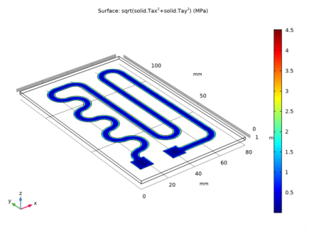
In the Settings window for Surface, click Replace Expression in the upper-right corner of the Expression section. From the menu, choose Component 1>Electric Currents in Layered Shells>Heating and losses>ecis.Qsh - Surface loss density, electromagnetic - W/m².
|
|
3
|
|
4
|
|
5
|
|
1
|
|
2
|
|
3
|
|
1
|
|
2
|
|
3
|
|
4
|
|
5
|
|
1
|
|
1
|
|
2
|
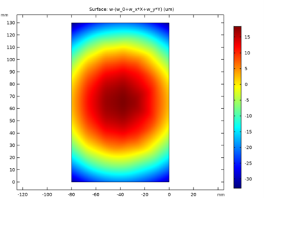
In the Settings window for 2D Plot Group, type Displacement, Bottom Boundary in the Label text field.
|
|
1
|
|
2
|
In the Settings window for Surface, click Replace Expression in the upper-right corner of the Expression section. From the menu, choose Component 1>Solid Mechanics>Displacement>solid.disp - Total displacement - m.
|
|
3
|
|
4
|
|
1
|
|
2
|
|
3
|
|
5
|
|
1
|
|
2
|
|
3
|
|
4
|
Browse to the model’s Application Libraries folder and double-click the file heating_circuit_variables.txt.
|
|
5
|
|
6
|
In the Show More Options dialog box, in the tree, select the check box for the node General>Variable Utilities.
|
|
7
|
Click OK.
|
|
1
|
|
2
|
|
3
|
|
1
|
|
2
|
|
3
|
|
4
|
|
1
|
|
3
|
In the Settings window for Surface Integration, click Replace Expression in the upper-right corner of the Expressions section. From the menu, choose Component 1>Heat Transfer in Solids>Boundary fluxes>ht.q0 - Inward heat flux - W/m².
|
|
4
|
Click Evaluate.
|
|
1
|
Go to the Table window.
|
|
1
|
|
2
|
|
3
|
|
4
|
Click Replace Expression in the upper-right corner of the Expressions section. From the menu, choose Component 1>Electric Currents in Layered Shells>Heating and losses>ecis.Qsh - Surface loss density, electromagnetic - W/m².
|
|
5
|
Click Evaluate.
|
|
1
|
Go to the Table window.
|