PDF

Frequency Domain Modeling of a Capacitor
Introduction
A capacitor with an applied sinusoidally time-varying voltage difference is modeled. A wide frequency range is considered and the impedance of the device is computed. Solver accuracy is addressed. The relationship between the frequency domain impedance and the steady-state capacitance and resistance of the device is discussed.
Figure 1: A simple capacitor composed of a disk of dielectric with metal plates on either side, and lead wires. An AC signal is applied.
Model Definition
The capacitor being modeled is shown in Figure 1, two metal disks, with leads, are separated by a disk of quartz glass with relative permittivity εr = 4.2 and a small electric conductivity σ = 10-14  S/m. A region of surrounding air (εr = 1.0, σ = 0 S/m) is also modeled to account for the fringing fields. A sinusoidally time-varying 10 kV source is connected to the leads and the electric potential distribution and admittance of the device is computed.
It is assumed that the capacitor plates are made of a highly conductive material, that their total effective resistivity is much lower than that of the quartz. It is further assumed that the absolute magnitude of the current flow is small, which implies negligible magnetic fields and magnetically induced currents. Under these assumptions, the terminals can be assumed to be equipotential at any instant in time.
A separate electrostatic analysis can be used to compute the capacitance of the device, C. Similarly, a separate Stationary Electric Currents analysis can be used to compute the conductance of the cylinder of quartz, G. Under the previous assumptions, and for a device with no frequency-dependent material properties, the admittance can be computed from:
Where ω is the angular frequency of excitation. It can be observed from this equation that as the frequency increases, the imaginary component of the admittance, the capacitive contribution, becomes many orders of magnitude larger than the real component, the conductive contribution.
In such cases, where the model is dominated by either conductive or capacitive effects, it can become necessary to change the default solver settings. The default solver for 3D electromagnetic problems uses an iterative approach, which means that the solution is found to within a relative tolerance. The default relative tolerance for the iterative solver is 10-3, but this can be tightened up to 10-6 if needed. Beyond a relative tolerance of 10-6 it may become difficult for the iterative solver to converge. If even higher accuracy is needed, it is also possible to use a direct solver, although this does take more time and memory to solve. Both iterative and direct solvers are used, and compared.
Results and Discussion
The electric potential is plotted in Figure 2. The admittance is computed and the real and imaginary components of the admittance are shown to be related to the steady state conductance and capacitance. When using the iterative solver, and as the capacitive effects begin to dominate the admittance, the conductive component of the admittance becomes less accurate. Once the real component of the admittance is less than six orders of magnitude smaller than the imaginary component, the results are below the tolerance threshold of the iterative solver, and the real component of the admittance is no longer accurate. Using the direct solver can improve this accuracy, if desired.
Irrespective of the solver used, and the tolerance specified, the dominant component of the admittance is computed correctly. This device is primarily capacitive, and such capacitive behavior is captured correctly, even with the default solver settings. The total resistive losses within the dielectric, are also computed correctly, regardless of solution method.
Figure 2: The electric field strength and resistive losses in the dielectric and air domain surrounding the capacitor.
Application Library path: ACDC_Module/Capacitive_Devices/capacitor_ac
Modeling Instructions
From the File menu, choose New.
New
In the New window, click Model Wizard.
Model Wizard
1
In the Model Wizard window, click 3D.
2
In the Select Physics tree, select AC/DC>Electric Fields and Currents>Electric Currents (ec).
3
Click Add.
4
Click Study.
5
In the Select Study tree, select General Studies>Frequency Domain.
6
Click Done.
Geometry 1
1
In the Model Builder window, under Component 1 (comp1) click Geometry 1.
2
In the Settings window for Geometry, locate the Units section.
3
From the Length unit list, choose cm.
First, create a cylinder for the model domain.
Cylinder 1 (cyl1)
1
In the Geometry toolbar, click Cylinder.
2
In the Settings window for Cylinder, locate the Size and Shape section.
3
In the Radius text field, type 20.
4
In the Height text field, type 20.
5
Click Build Selected.
Choose wireframe rendering to get a better view of the interior parts.
6
Click the Wireframe Rendering button in the Graphics toolbar.
Then, add a cylinder for the disc of dielectric with the two metal plates.
Cylinder 2 (cyl2)
1
In the Geometry toolbar, click Cylinder.
2
In the Settings window for Cylinder, locate the Size and Shape section.
3
In the Radius text field, type 10.
4
In the Height text field, type 4.
5
Locate the Position section. In the z text field, type 8.
6
Click to expand the Layers section. In the table, enter the following settings:
7
Clear the Layers on side check box.
8
Select the Layers on bottom check box.
9
Select the Layers on top check box.
Finish the geometry by adding two cylinders for the leads.
Cylinder 3 (cyl3)
1
In the Geometry toolbar, click Cylinder.
2
In the Settings window for Cylinder, locate the Size and Shape section.
3
In the Radius text field, type 0.75.
4
In the Height text field, type 8.
5
Click Build Selected.
Cylinder 4 (cyl4)
1
Right-click Cylinder 3 (cyl3) and choose Duplicate.
2
In the Settings window for Cylinder, locate the Position section.
3
In the z text field, type 12.
4
Click Build All Objects.
Electric Currents (ec)
The model is composed of a disc of dielectric material with metal plates on either side and two lead wires. To get a better view, hide some of the boundaries. Begin by selecting the Electric Currents interface, then add a Hide node.
Definitions
Hide for Physics 1
1
In the Model Builder window, expand the Component 1 (comp1)>Definitions node.
2
Right-click View 1 and choose Hide for Physics.
3
In the Settings window for Hide for Physics, locate the Geometric Entity Selection section.
4
From the Geometric entity level list, choose Boundary.
5
Even though not strictly necessary for a closed electrode, the domains inside the ground surfaces are disabled with the next instructions. This is the suggested model setup whenever the electrode is considered to be equipotential as this is excluding any possible numerical issue due to the effect of the large contrast in material properties.
Electric Currents (ec)
1
In the Model Builder window, under Component 1 (comp1) click Electric Currents (ec).
2
Terminal 1
1
In the Physics toolbar, click Domains and choose Terminal.
2
3
In the Settings window for Terminal, locate the Terminal section.
4
From the Terminal type list, choose Voltage.
5
In the V0 text field, type 10[kV].
Explicit 1
1
In the Definitions toolbar, click Explicit.
2
3
In the Settings window for Explicit, locate the Output Entities section.
4
From the Output entities list, choose Adjacent boundaries.
Electric Currents (ec)
Ground 1
1
In the Physics toolbar, click Boundaries and choose Ground.
2
In the Settings window for Ground, locate the Boundary Selection section.
3
From the Selection list, choose Explicit 1.
Next, assign material properties to the model. Begin by specifying Air for all domains.
Add Material
1
In the Home toolbar, click Add Material to open the Add Material window.
2
Go to the Add Material window.
3
4
Click Add to Component in the window toolbar.
Override the dielectric disc with glass (quartz).
5
Go to the Add Material window.
6
In the tree, select Built-in>Glass (quartz).
7
Click Add to Component in the window toolbar.
8
In the Home toolbar, click Add Material to close the Add Material window.
Materials
Glass (quartz) (mat2)
Select Domain 3 only.
Mesh 1
1
In the Model Builder window, under Component 1 (comp1) click Mesh 1.
2
In the Settings window for Mesh, click Build All.
Study 1
1
In the Model Builder window, click Study 1.
2
In the Settings window for Study, locate the Study Settings section.
3
Clear the Generate default plots check box.
Step 1: Frequency Domain
1
In the Model Builder window, under Study 1 click Step 1: Frequency Domain.
2
In the Settings window for Frequency Domain, locate the Study Settings section.
3
In the Frequencies text field, type 1 10 100 1000 10000 100000.
Solution 1 (sol1)
1
In the Study toolbar, click Show Default Solver.
2
In the Model Builder window, expand the Solution 1 (sol1) node, then click Stationary Solver 1.
3
In the Settings window for Stationary Solver, locate the General section.
4
In the Relative tolerance text field, type 1e-6.
5
In the Study toolbar, click Compute.
Add a Selection to the first solution. This selection will only include the air and the glass. Domains that are excluded from the selection will be hidden in the corresponding plots.
Results
In the Model Builder window, expand the Results node.
Study 1/Solution 1 (sol1)
In the Model Builder window, expand the Results>Datasets node, then click Study 1/Solution 1 (sol1).
Selection
1
In the Results toolbar, click Attributes and choose Selection.
2
In the Settings window for Selection, locate the Geometric Entity Selection section.
3
From the Geometric entity level list, choose Domain.
4
Add a duplicate solution and set a selection for the metal parts.
Study 1/Solution 1 (2) (sol1)
In the Results toolbar, click More Datasets and choose Solution.
Selection
1
In the Results toolbar, click Attributes and choose Selection.
2
In the Settings window for Selection, locate the Geometric Entity Selection section.
3
From the Geometric entity level list, choose Domain.
4
3D Plot Group 1
In the Results toolbar, click 3D Plot Group.
The metal parts can be visualized by choosing Uniform for the coloring type. In this case the purpose of the plot is not to show a quantity, but to show a shape. The variable that the plot is based on is of no importance. Create a surface plot for this purpose.
Surface 1
1
Right-click 3D Plot Group 1 and choose Surface.
2
In the Settings window for Surface, locate the Data section.
3
From the Dataset list, choose Study 1/Solution 1 (2) (sol1).
4
Locate the Coloring and Style section. From the Coloring list, choose Uniform.
5
From the Color list, choose Gray.
Add slice plots for the norm of the electric potential and resistive losses.
Slice 1
1
In the Model Builder window, right-click 3D Plot Group 1 and choose Slice.
2
In the Settings window for Slice, locate the Plane Data section.
3
In the Planes text field, type 1.
4
Locate the Coloring and Style section. From the Color table list, choose RainbowLight.
Slice 2
1
Right-click 3D Plot Group 1 and choose Slice.
2
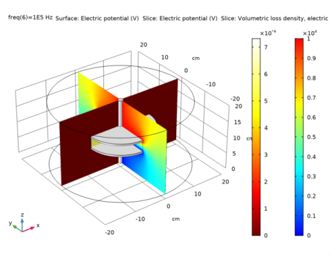
In the Settings window for Slice, click Replace Expression in the upper-right corner of the Expression section. From the menu, choose Component 1>Electric Currents>Heating and losses>ec.Qrh - Volumetric loss density, electric - W/m³.
3
Locate the Plane Data section. From the Plane list, choose ZX-planes.
4
In the Planes text field, type 1.
5
Locate the Coloring and Style section. From the Color table list, choose ThermalLight.
6
In the 3D Plot Group 1 toolbar, click Plot.
Compare the resulting plot with that in Figure 2.
Global Evaluation 1
1
In the Results toolbar, click Global Evaluation.
2
In the Settings window for Global Evaluation, locate the Expressions section.
3
4
Click Evaluate.
Global Evaluation 2
1
In the Results toolbar, click Global Evaluation.
2
In the Settings window for Global Evaluation, locate the Expressions section.
3
4
Click Evaluate.
Volume Integration 1
1
In the Results toolbar, click More Derived Values and choose Integration>Volume Integration.
2
3
In the Settings window for Volume Integration, locate the Expressions section.
4
5
Click Evaluate.
Study 1
Next, use the direct solver to improve the accuracy of the conductive component of the admittance.
Solution 1 (sol1)
1
In the Model Builder window, expand the Study 1>Solver Configurations>Solution 1 (sol1)>Stationary Solver 1 node.
2
Right-click Study 1>Solver Configurations>Solution 1 (sol1)>Stationary Solver 1>Direct and choose Enable.
3
In the Home toolbar, click Compute.
Results
Global Evaluation 1
1
In the Model Builder window, under Results>Derived Values click Global Evaluation 1.
2
Click Evaluate.
Global Evaluation 2
1
In the Model Builder window, click Global Evaluation 2.
2
Click Evaluate.
Volume Integration 1
1
In the Model Builder window, click Volume Integration 1.
2
Click Evaluate.
3D Plot Group 1
Now, compare the values in Table 1. Set the table to Full Precision using the buttons in the tables toolbar. The real part of the admittance should be much more consistent at higher frequencies when using the direct solver. For the capacitance and the resistive losses, the difference is less prominent (see Table 2 and Table 3).