PDF

Thickness Shear Mode Quartz Oscillator
Introduction
AT cut quartz crystals are widely employed in a range of applications, from oscillators to microbalances. One of the important properties of the AT cut is that the resonant frequency of the crystal is temperature independent to first order. This is desirable in both mass sensing and timing applications. AT cut crystals vibrate in the thickness shear mode — an applied voltage across the faces of the cut produces shear stresses inside the crystal. This example considers the vibration of an AT cut thickness shear oscillator, focusing on the mechanical response of the system in the frequency domain. The effect of a series capacitor on the mechanical resonance is also considered. Adding a series capacitance is a technique frequently employed to tune crystal oscillators.
Model Definition
The model geometry is shown in Figure 1. The oscillator consists of a single (left-handed) quartz disc, supported so as not to impede the motion of the vibrational mode. There are two electrodes on the top and bottom surfaces of the geometry, one of which is grounded.
Figure 1: Model geometry.
In the first version of the model an AC voltage is applied to the top electrode. In the second version, the crystal is still driven by an AC voltage, but a capacitor is placed between the voltage source and the top electrode of the crystal.
Domain Level Equations
Within a piezoelectric crystal there is a coupling between the strain and the electric field, which is determined by the constitutive relation:
(1)
Here, S is the strain, T is the stress, E is the electric field, and D is the electric displacement field. The material parameters cE, e, and εS, correspond to the material stiffness, the coupling properties, and the permittivity. These quantities are tensors of rank 4, 3, and 2 respectively, but, since the tensors are highly symmetric for physical reasons, they can be represented as matrices within an abbreviated subscript notation, which is usually more convenient. Equation 1 is implemented by the Piezoelectric Effect branch located under the Multiphysics branch. This constitutive relation is used to couple the equations of Solid Mechanics and Electrostatics, which are solved within the material.
Material Orientation
The orientation of a piezoelectric crystal cut is frequently defined by the system introduced by the IRE standard of 1949 (Ref. 1). This standard has undergone a number of subsequent revisions, with the final revision being the IEEE standard of 1987 (Ref. 2). Unfortunately the 1987 standard contained a number of serious errors and the IEEE subsequently withdrew it. COMSOL Multiphysics therefore adopts the preceding 1978 standard (Ref. 3), which is similar to the 1987 standard, for material property definitions. Most of the material properties in the material library are based on the values given in the book by Auld (Ref. 4), which uses the 1978 IEEE conventions. This is consistent with general practice except in the specific case of Quartz, where it is more common to use the 1949 IRE standard to define the material properties. COMSOL Multiphysics therefore provides an additional set of material properties consistent with the 1949 standard for the case of Quartz. Note that the material properties for quartz are based on Ref. 5, which uses the 1949 IRE standard (the properties are appropriately modified according to the different standards).
The stiffness, compliance, coupling, and dielectric material property matrices are defined with the crystal axes aligned with the local coordinate axes. Note that the signs of several matrix components differ between the IRE 1949 and the IEEE 1978 standards (see Table 1). In the absence of a user-defined coordinate system, the local system corresponds to the global X, Y, and Z coordinate axes. When an alternative coordinate system is selected this system defines the orientation of the crystal axes. This is the mechanism used in COMSOL Multiphysics to define a particular crystal cut, and typically it is necessary to calculate the appropriate Euler angles for the cut (given the thickness orientation for the wafer). All piezoelectric material properties are defined using the Voigt form of the abbreviated subscript notation, which is universally employed in the literature (this differs from the standard notation used for Linear Elastic Material in the Solid Mechanics interface). The material properties are defined in the material frame, so that if the solid rotates during deformation the material properties rotate with the solid.
Crystal cuts are usually defined by a mechanism introduced by the IEEE/IRE standards. Both standards use a notation that defines the orientation of a virtual slice (the plate) through the crystal. The crystal axes are denoted X, Y, and Z and the plate, which is usually rectangular, is defined as having sides l, w, and t (length, width, and thickness). Initially the plate is aligned with respect to the crystal axes and then up to three rotations are defined, using a right-handed convention about axes embedded along the l, w, and t sides of the plate. This model uses AT cut quartz, defined in the IEEE 1978 standard as: (YXl) 35.25°. The first two letters in the bracketed expression always refer to the initial orientation of the thickness and the length of the plate. Subsequent bracketed letters then define up to three rotational axes, which move with the plate as it is rotated. Angles of rotation about these axes are specified after the bracketed expression in the order of the letters, using a right-handed convention. For AT cut quartz only one rotation, about the l axis, is required. This is illustrated in Figure 2. Note that within the 1949 IRE Standard AT cut quartz is denoted as: (YXl) +35.25°. Table 2 summarizes the differences between the standards for the AT cut.
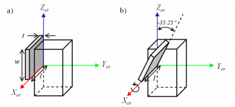
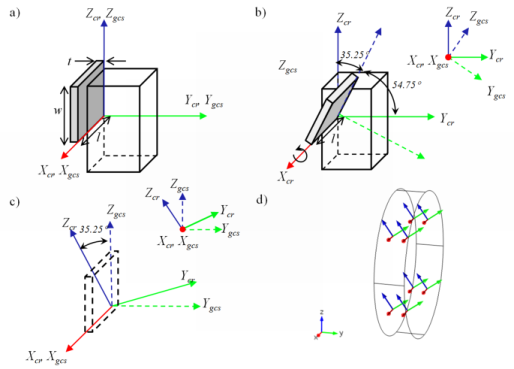
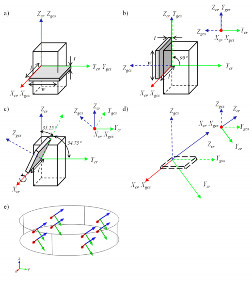
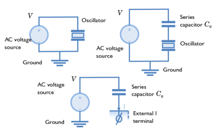
When defining the material properties of Quartz, the orientation of the X, Y, and Z axes with respect to the crystal differs between the 1978 IEEE standard and the 1949 IRE standard. A consequence of this is that both the material property matrices and the crystal cuts differ between the two standards. Table 1 summarizes the signs for the important matrix elements under the two conventions. Table 2 shows the different definitions of the crystal cuts under the two conventions.
s14
c14
d11
d14
e11
e14
(ZXZ: 0°,−35.25°,0°)
(ZXZ: 0°,125.25°,0°)
(ZXZ: 0°, 35.25°,0°)
(ZXZ: 0°,-54.75°,0°)
When defining the material orientation it is necessary to consider the orientation of the plate with respect to the global coordinate system in addition to the orientation of the plate with respect to the crystallographic axes.
This model uses AT cut quartz, defined in the IEEE 1978 standard as shown in Figure 2. The definition of the appropriate local coordinate system depends on the desired final orientation of the plate in the global coordinate system. One way to set up the plate is to orientate its normal parallel to the Y axis in the global coordinate system. Figure 3 shows how to define the local coordinate system in this case (instructions for how to set up the crystal in this manner are provided in brackets in the step by step instructions).
Figure 4 shows how to define the local system such that the plate has its normal parallel to the global Z axis, which is the case for the crystal in this model.
Whatever crystal orientation is chosen, it is critical to keep track of the orientation of the local system with respect to the global system, which is defined depending on the desired orientation of the plate in the model.
There are also a number of methods to define the local coordinate system with respect to the global system. Usually it is most convenient to define the local coordinates with a Rotated System node, which defines three Euler angles according to the ZXZ convention (rotation about Z, then X, then Z again). Note that these Euler angles define the local (crystal) axes with respect to the global axes — this is distinct from the approach of defining the cut (global) axes with respect to the crystal (local) axes.
Figure 2: Definition of the AT cut of quartz within the IEEE 1978 standard. The AT cut is defined as: (YXl) 35.25°. The first two bracketed letters specify the initial orientation of the plate, with the thickness direction, t, along the crystal Y axis and the length direction, l, along the X axis. Then up to three rotations about axes that move with the plate are specified by the corresponding bracketed letters and the subsequent angles. In this case only one rotation is required about the l axis, of 35.25° (in a right-handed sense).
Figure 3: Defining an AT cut crystal plate within COMSOL Multiphysics, with normal in the global Y-direction. Within the 1978 IEEE standard the AT cut is defined as (YXl) -35.25°. Start with the plate normal or thickness in the Ycr direction (a) and rotate the plate 35.25° about the l axis (b). The global coordinate system rotates with the plate. Finally rotate the entire system so that the global coordinate system is orientated as it appears in COMSOL Multiphysics (c). The local coordinate system should be defined with the Euler angles (ZXZ - 0, 35.25°, 0).(d) shows a coordinate system for this system in COMSOL Multiphysics.
Figure 4: Defining an AT cut crystal plate within COMSOL Multiphysics, with normal in the global Z-direction. Within the 1978 IEEE standard the AT cut is defined as (YXl) 35.25°. Begin with the plate normal in the Zcr-direction, so the crystal and global systems are coincident. Rotate the plate so that its thickness points in the Ycr-direction (the starting point for the IEEE definition), the global system rotates with the plate (b). Rotate the plate 35.25° about the l axis (d). Finally rotate the entire system so that the global coordinate system is orientated as it appears in COMSOL Multiphysics (d). The local coordinate system should be defined with the Euler angles (ZXZ: 0, -54.75°, 0). (e) shows a coordinate system for this system in COMSOL Multiphysics.
Electrical Circuit
In the first part of the model an AC voltage is applied directly to the top plate of the oscillator, which is grounded. In the second part of the model, a capacitor is added between the voltage source and the oscillator, as shown in Figure 5. In COMSOL Multiphysics, the oscillator is coupled into the circuit using the External I Terminal feature. The terminal boundary condition within the model is set to Circuit and this feature then captures the charge generated by the circuit.
Figure 5: Top left: Electrical circuit for the first part of the model. Top right: Electrical circuit for the second part of the model. Bottom: Circuit for the second part of the model as implemented in COMSOL Multiphysics.
Results and Discussion
Figure 6 shows the crystal displacement at its resonant frequency of 5.11 MHz. The form of the displacement shows clearly the shear nature of the resonance. The potential on cut slices through the plate is illustrated in Figure 7. The mechanical domain frequency response of the oscillator is shown in Figure 8. A clear anti-resonance is apparent, with a resonant frequency close to 5.11 MHz.
The addition of a series capacitance between the oscillator and the voltage source is expected to pull the resonant frequency to higher values. Figure 9 shows that this effect occurs as expected, with the resonant frequency increasing the most for smaller values of the series capacitance (in the limit of very large series capacitance the impedance of the series capacitor goes to zero and produces the result shown in Figure 8).
Figure 6: Displacement of the crystal at resonance.
Figure 7: Electric potential inside the crystal at resonance.
Figure 8: Mechanical response of the structure with no series capacitance.
Figure 9: Mechanical response of the structure with different series capacitances.
References
1. “Standards on Piezoelectric Crystals, 1949”, Proceedings of the I. R. E.,vol. 37, no.12, pp. 1378–1395, 1949.
2. IEEE Standard on Piezoelectricity, ANSI/IEEE Standard 176-1987, 1987.
3. IEEE Standard on Piezoelectricity, ANSI/IEEE Standard 176-1978, 1978.
4. B. A. Auld, Acoustic Fields and Waves in Solids, Krieger Publishing Company, 1990.
5. R. Bechmann, “Elastic and Piezoelectric Constants of Alpha-Quartz”, Physical Review B, vol. 110 no. 5, pp. 1060–1061, 1958.
Application Library path: MEMS_Module/Piezoelectric_Devices/thickness_shear_quartz_oscillator
Modeling Instructions
From the File menu, choose New.
New
In the New window, click Model Wizard.
Model Wizard
1
In the Model Wizard window, click 3D.
2
In the Select Physics tree, select Structural Mechanics>Piezoelectric Devices.
3
Click Add.
4
Click Study.
5
In the Select Study tree, select Preset Studies for Selected Physics Interfaces>Frequency Domain.
6
Click Done.
Global Definitions
Add parameters for the model geometry and series capacitance.
Parameters
1
On the Home toolbar, click Parameters.
2
In the Settings window for Parameters, locate the Parameters section.
3
Geometry 1
Create the geometry.
Cylinder 1 (cyl1)
1
On the Geometry toolbar, click Cylinder.
2
In the Settings window for Cylinder, locate the Size and Shape section.
3
In the Radius text field, type R0.
4
In the Height text field, type H0.
If you wish to set up the material orientation using the alternative method shown in Figure 3, change the Axis type to y-axis.
5
Click Build All Objects.
Definitions
Set up a rotated system appropriate for AT cut Quartz.
Rotated System 2 (sys2)
1
On the Definitions toolbar, click Coordinate Systems and choose Rotated System.
2
In the Settings window for Rotated System, locate the Settings section.
3
Find the Euler angles (Z-X-Z) subsection. In the β text field, type -54.75[deg].
If you wish to set up the material orientation using the alternative method shown in Figure 3, type 35.25[deg] in the β text field.
Add Material
1
On the Home toolbar, click Add Material to open the Add Material window.
2
Go to the Add Material window.
3
In the tree, select Piezoelectric>Quartz LH (1978 IEEE).
4
Click Add to Component in the window toolbar.
Materials
Quartz LH (1978 IEEE) (mat1)
On the Home toolbar, click Add Material to close the Add Material window.
Solid Mechanics (solid)
Use the rotated system to define the orientation of the crystal.
Piezoelectric Material 1
1
In the Model Builder window, under Component 1 (comp1)>Solid Mechanics (solid) click Piezoelectric Material 1.
2
In the Settings window for Piezoelectric Material, locate the Coordinate System Selection section.
3
From the Coordinate system list, choose Rotated System 2 (sys2).
Add damping to the model.
Mechanical Damping 1
1
Right-click Component 1 (comp1)>Solid Mechanics (solid)>Piezoelectric Material 1 and choose Damping.
2
In the Settings window for Mechanical Damping, locate the Damping Settings section.
3
From the Damping type list, choose Isotropic loss factor.
4
From the ηs list, choose User defined. In the associated text field, type 1e-3.
Electrostatics (es)
Add electrical boundary conditions to the model. First add a Terminal boundary condition that connects the electrode to an external circuit.
Terminal 1
1
In the Model Builder window, under Component 1 (comp1) right-click Electrostatics (es) and choose the boundary condition Terminal.
2
3
In the Settings window for Terminal, locate the Terminal section.
4
From the Terminal type list, choose Circuit.
Over-ride the preceding boundary condition with a constant potential boundary condition to compute the response of the device without a series capacitance. This node will be disabled in the study when the circuit is included in the model.
Terminal 2
1
In the Model Builder window, right-click Electrostatics (es) and choose the boundary condition Terminal.
2
In the Settings window for Terminal, locate the Terminal section.
3
In the Terminal name text field, type 1.
4
5
From the Terminal type list, choose Voltage.
6
In the V0 text field, type 10.
Ground 1
1
Right-click Electrostatics (es) and choose Ground.
2
Root
In the second study in this model, the effect of a series capacitor on the device response will be investigated. Add an Electrical Circuit interface to model the capacitor.
Add Physics
1
On the Home toolbar, click Add Physics to open the Add Physics window.
2
Go to the Add Physics window.
3
In the tree, select AC/DC>Electrical Circuit (cir).
4
Click Add to Component in the window toolbar.
5
On the Home toolbar, click Add Physics to close the Add Physics window.
Electrical Circuit (cir)
Features in the Electric Circuits interface are connected by specifying connecting node numbers for each port of the device.
Ground Node 1
A ground node is automatically added to the circuit, with the default node number of 0.
Next add a voltage source between the ground node and a (newly created) node with number 2.
Voltage Source V1
1
In the Model Builder window, right-click Electrical Circuit (cir) and choose Voltage Source.
2
In the Settings window for Voltage Source, locate the Node Connections section.
3
4
Locate the Device Parameters section. From the Source type list, choose AC-source.
5
In the Vsrc text field, type 10.
Add a capacitor between the voltage source output (node 2) and a new node, 1.
Capacitor C1
1
Right-click Electrical Circuit (cir) and choose Capacitor.
2
In the Settings window for Capacitor, locate the Node Connections section.
3
4
Locate the Device Parameters section. In the C text field, type Cs.
Connect node 1 to the Terminal feature in the model using the External I-Terminal feature.
External I-Terminal 1
1
Right-click Electrical Circuit (cir) and choose External Couplings>External I-Terminal.
Couple the electric potential from the Terminal in the electrostatics interface back into the model.
2
In the Settings window for External I-Terminal, locate the Node Connections section.
3
In the Node name text field, type 1.
4
Locate the External Terminal section. From the V list, choose Terminal voltage (es).
Mesh 1
Create a swept triangular mesh.
Free Triangular 1
1
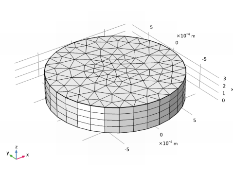
In the Model Builder window, under Component 1 (comp1) right-click Mesh 1 and choose More Operations>Free Triangular.
2
Distribution 1
1
In the Model Builder window, right-click Mesh 1 and choose Swept.
2
Right-click Swept 1 and choose Distribution.
3
In the Settings window for Distribution, locate the Distribution section.
4
In the Number of elements text field, type 4.
5
Click Build All.
The mesh used here is somewhat coarse for the range of frequencies that are solved for. This is mainly to keep the computational time and RAM requirements as low as possible. Interested users are encouraged to solve the problem for finer mesh settings.
Study 1
Set up and solve a frequency dependent study.
Step 1: Frequency Domain
1
In the Model Builder window, under Study 1 click Step 1: Frequency Domain.
2
In the Settings window for Frequency Domain, locate the Study Settings section.
3
Click Range.
4
In the Range dialog box, type 5.095[MHz] in the Start text field.
5
In the Step text field, type 1[kHz].
6
In the Stop text field, type 5.13[MHz].
7
Click Replace.
In the first study, disable the electrical circuit.
8
In the Settings window for Frequency Domain, locate the Physics and Variables Selection section.
9
In the table, clear the Solve for check box for the Electrical Circuit (cir) interface.
10
On the Home toolbar, click Compute.
Results
Instead of the stress plot, visualize the mode shape of the device at resonance. Note that this plot and subsequent plots will appear rotated compared to that shown in Figure 6 if the alternative definition of the material orientation described in Figure 3 is used.
Stress (solid)
1
In the Model Builder window, under Results click Stress (solid).
2
In the Settings window for 3D Plot Group, type Displacement in the Label text field.
3
Locate the Data section. From the Parameter value (freq (Hz)) list, choose 5.112E6.
Surface 1
1
In the Model Builder window, expand the Results>Displacement node, then click Surface 1.
2
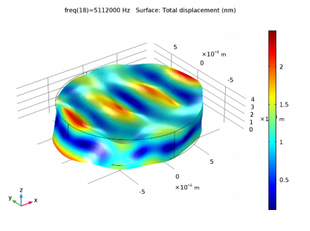
In the Settings window for Surface, click Replace Expression in the upper-right corner of the Expression section. From the menu, choose Component 1>Solid Mechanics>Displacement>solid.disp - Total displacement.
3
Locate the Expression section. From the Unit list, choose nm.
4
Click the Zoom Extents button on the Graphics toolbar.
5
On the Displacement toolbar, click Plot.
The second default plot shows the electric potential within the device. For a better view, plot 5 slices in xy planes.
Electric Potential (es)
1
In the Model Builder window, under Results click Electric Potential (es).
2
In the Settings window for 3D Plot Group, locate the Data section.
3
From the Parameter value (freq (Hz)) list, choose 5.112E6.
Multislice 1
1
In the Model Builder window, expand the Electric Potential (es) node, then click Multislice 1.
2
In the Settings window for Multislice, locate the Multiplane Data section.
3
Find the x-planes subsection. In the Planes text field, type 5.
4
Find the y-planes subsection. In the Planes text field, type 0.
5
Find the z-planes subsection. In the Planes text field, type 0.
6
On the Electric Potential (es) toolbar, click Plot.
Add a plot to show the mechanical response of the device.
1D Plot Group 3
1
On the Home toolbar, click Add Plot Group and choose 1D Plot Group.
2
In the Settings window for 1D Plot Group, type Mechanical Response in the Label text field.
Point Graph 1
1
Right-click Mechanical Response and choose Point Graph.
2
3
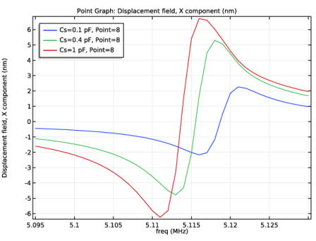
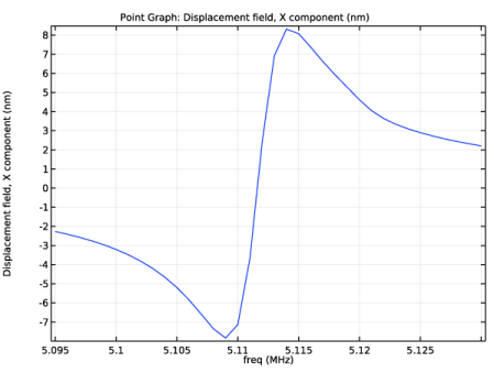
In the Settings window for Point Graph, click Replace Expression in the upper-right corner of the y-axis data section. From the menu, choose Component 1>Solid Mechanics>Displacement>Displacement field (material and geometry frames)>u - Displacement field, X component.
4
Locate the y-Axis Data section. From the Unit list, choose nm.
5
Locate the x-Axis Data section. From the Unit list, choose MHz.
6
On the Mechanical Response toolbar, click Plot.
Now set up a study to compute the frequency response of the device with different capacitors added in series.
Add Study
1
On the Home toolbar, click Add Study to open the Add Study window.
2
Go to the Add Study window.
3
Find the Studies subsection. In the Select Study tree, select Preset Studies>Frequency Domain.
4
Click Add Study in the window toolbar.
5
On the Home toolbar, click Add Study to close the Add Study window.
Study 2
Step 1: Frequency Domain
1
In the Model Builder window, under Study 2 click Step 1: Frequency Domain.
2
In the Settings window for Frequency Domain, locate the Study Settings section.
3
Click Range.
4
In the Range dialog box, type 5.095[MHz] in the Start text field.
5
In the Step text field, type 1[kHz].
6
In the Stop text field, type 5.13[MHz].
7
Click Replace.
8
In the Settings window for Frequency Domain, locate the Physics and Variables Selection section.
9
Select the Modify physics tree and variables for study step check box.
10
In the Physics and variables selection tree, select Component 1 (comp1)>Electrostatics (es)>Terminal 2.
11
Click Disable.
Parametric Sweep
1
On the Study toolbar, click Parametric Sweep.
2
In the Settings window for Parametric Sweep, locate the Study Settings section.
3
Click Add.
4
5
In the Model Builder window, click Study 2.
6
In the Settings window for Study, locate the Study Settings section.
7
Clear the Generate default plots check box.
8
On the Study toolbar, click Compute.
Results
Re-plot the mechanical response with the additional series capacitance.
Mechanical Response 1
1
In the Model Builder window, under Results right-click Mechanical Response and choose Duplicate.
2
In the Settings window for 1D Plot Group, type Mechanical response, Parametric in the Label text field.
3
Locate the Data section. From the Data set list, choose Study 2/Parametric Solutions 1 (sol3).
4
Click to expand the Legend section. From the Position list, choose Upper left.
Point Graph 1
1
In the Model Builder window, expand the Results>Mechanical response, Parametric node, then click Point Graph 1.
2
In the Settings window for Point Graph, click to expand the Legends section.
3
Select the Show legends check box.
4
On the Mechanical response, Parametric toolbar, click Plot.
Note how the mechanical resonant frequency is ’pulled’ by the series capacitance.