PDF

Heat Transfer in a Surface-Mount Package for a Silicon Chip
Introduction
All integrated circuits—especially high-speed devices—produce heat. In today’s dense electronic system layouts heat sources are many times placed close to heat-sensitive ICs. Designers of printed-circuit boards often need to consider the relative placement of heat-sensitive and heat-producing devices, so that the sensitive ones do not overheat.
One type of heat-generating device is a voltage regulator, which can produce several watts of heat and reach a temperature higher than 70 °C. If the board design places such a device close to a surface-mounted package that contains a sensitive silicon chip, the regulator’s heat could cause reliability problems and failure due to overheating.
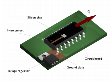
Figure 1: Layout of the simulated silicon device, its package, and a voltage regulator. The chip and the voltage regulator are connected through a ground plate, a pin, and the interconnect.
This simulation investigates the thermal situation for a silicon chip in a surface-mount package placed on a circuit board close to a hot voltage regulator. The chip is subjected to heat from the regulator and from internally generated heat.
Model Definition
The model is based on a SMD IC and voltage regulator layout as in Figure 1. The silicon chip sits in the center of the package and dissipates its heat to the surrounding environments. The chip also connects to a ground plane through an interconnect and one of the pins. A heat generating voltage regulator is placed on the same ground plane. This means that the voltage regulator may affect the silicon chip by the conducted heat and this may lead to overheating of the chip.
Heat transfers through the mount package to the surroundings through conduction according to:
The heat source, Q, is negligible in the circuit board, pins and package, while in the chip, this model sets that parameter to a value equivalent to 20 mW. The conductivities of the components are chosen to be similar to:
Heat dissipates from all air-exposed surfaces through forced heat convection, which is modeled using a heat transfer coefficient, h:
The voltage regulator is simulated by setting a fixed temperature at that surface. The thin conducting layers of the ground plane and interconnect within the package is modeled using a 2D shell approximation, according to:
where ds is the layer’s thickness, and t represents the nabla operator projected onto the direction of the plane. The model uses a Heat Transfer interface to describe the 3D heat transfer as well as the 2D shell heat transfer.
Results and Discussions
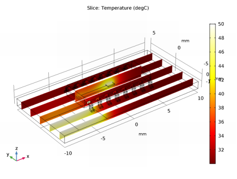
Figure 2 illustrates the temperature distribution through the thickness. Being a good conductor, the interconnect delivers heat to the outer edge of the package, which gives the fairly constant temperature distribution around the interconnect.
Figure 2: Slice plot of the temperature through the circuit board, interconnect, chip, and package. The effect of the interconnect is evident by its ability to conduct heat from the chip to the outer parts of the package.
An alternative view is achieved by using the transparency feature in the visualization tools of COMSOL Multiphysics. This results in a transparent 3D view of the temperature distribution, as shown in Figure 3. In that figure you can see the temperature distribution around the chip and along the interconnect.
Figure 3: Boundary plot of the temperature created with the assistance of the transparency tool in COMSOL Multiphysics. This view also gives the temperature distribution on the chip and along the interconnect.
To get a closer look at the stationary temperature of the silicon chip, plot the temperature at the bottom boundary of the chip.
Figure 4: Temperature distribution on the bottom surface of the silicon chip.
The simulation predicts a maximum temperature of the silicon device of 47.7 °C. This means that the device does not overheat in the present configuration.
Application Library path: Heat_Transfer_Module/Power_Electronics_and_Electronic_Cooling/surface_mount_package
Notes About the COMSOL Implementation
This tutorial uses the Heat Transfer interface from the Heat Transfer Module and, in particular, its Thin Layer feature. These are thin layers that conduct heat well so you need not define them in 3D. The two layers that have this definition are:
While the numerical method considers these two modeling domains as interior boundaries, the model still includes a thickness to take the 3D heat flux into account.
Modeling Instructions
From the File menu, choose New.
New
In the New window, click Model Wizard.
Model Wizard
1
In the Model Wizard window, click 3D.
2
In the Select Physics tree, select Heat Transfer>Heat Transfer in Solids (ht).
3
Click Add.
4
Click Study.
5
In the Select Study tree, select Preset Studies>Stationary.
6
Click Done.
Geometry 1
The geometry sequence for the model is available in a file. If you want to create it from scratch yourself, you can follow the instructions in the Geometry Modeling Instructions section. Otherwise, insert the geometry sequence as follows:
1
On the Geometry toolbar, click Insert Sequence.
2
3
On the Geometry toolbar, click Build All.
4
Click the Zoom Extents button on the Graphics toolbar.
You should now see the geometry shown above.
The geometry includes the interconnect between the pin and the chip as well as the ground plate and the temperature surface resulting from the voltage regulator. To see the interconnect and the chip, you need to turn on transparency.
5
Click the Transparency button on the Graphics toolbar.
6
Click the Transparency button on the Graphics toolbar again to remove the transparency.
Now, define the domain settings including material properties, element order, heat source, and initial values.
Materials
To define material properties for the model domains, use four predefined materials from the Material Browser and one custom material.
Add Material
1
On the Home toolbar, click Add Material to open the Add Material window.
2
Go to the Add Material window.
3
In the tree, select Built-In>Aluminum.
4
Click Add to Component in the window toolbar.
5
In the Settings window for Material, locate the Geometric Entity Selection section.
6
From the Selection list, choose Pins.
Add Material
1
Go to the Add Material window.
2
In the tree, select Built-In>FR4 (Circuit Board).
3
Click Add to Component in the window toolbar.
Materials
FR4 (Circuit Board) (mat2)
1
In the Model Builder window, under Component 1 (comp1)>Materials click FR4 (Circuit Board) (mat2).
2
In the Settings window for Material, locate the Geometric Entity Selection section.
3
From the Selection list, choose PC Board.
Material 3 (mat3)
1
On the Materials toolbar, click Blank Material.
2
In the Settings window for Material, type Plastic in the Label text field.
3
Locate the Geometric Entity Selection section. From the Selection list, choose Chip Package.
Plastic (mat3)
1
In the Model Builder window, expand the Component 1 (comp1)>Materials>Plastic (mat3) node, then click Basic.
2
In the Settings window for Property Group, locate the Output Properties and Model Inputs section.
3
Find the Quantities subsection. In the tree, select Output Properties>Density.
4
Click Add.
5
Find the Output properties subsection. In the table, enter the following settings:
6
Find the Quantities subsection. In the tree, select Output Properties>Heat Capacity at Constant Pressure.
7
Click Add.
8
Find the Output properties subsection. In the table, enter the following settings:
9
Find the Quantities subsection. In the tree, select Output Properties>Thermal Conductivity.
10
Click Add.
11
Find the Output properties subsection. In the table, enter the following settings:
Add Material
1
Go to the Add Material window.
2
In the tree, select Built-In>Silicon.
3
Click Add to Component in the window toolbar.
Materials
Silicon (mat4)
1
In the Model Builder window, under Component 1 (comp1)>Materials click Silicon (mat4).
2
In the Settings window for Material, locate the Geometric Entity Selection section.
3
From the Selection list, choose Chip.
Add Material
1
Go to the Add Material window.
2
In the tree, select Built-In>Copper.
3
Click Add to Component in the window toolbar.
Materials
Copper (mat5)
1
In the Model Builder window, under Component 1 (comp1)>Materials click Copper (mat5).
2
In the Settings window for Material, locate the Geometric Entity Selection section.
3
From the Geometric entity level list, choose Boundary.
4
From the Selection list, choose Copper Layers.
5
On the Materials toolbar, click Add Material to close the Add Material window.
This completes the materials settings.
Heat Transfer in Solids (ht)
Heat Source 1
1
On the Physics toolbar, click Domains and choose Heat Source.
2
3
In the Settings window for Heat Source, locate the Heat Source section.
4
In the Q0 text field, type 2e8.
This completes the domain settings. Now, configure to the boundary conditions.
Heat Flux 1
1
On the Physics toolbar, click Boundaries and choose Heat Flux.
2
In the Settings window for Heat Flux, locate the Boundary Selection section.
3
From the Selection list, choose Exterior Boundaries.
4
Locate the Heat Flux section. Click the Convective heat flux button.
5
In the h text field, type 50.
6
In the Text text field, type 30[degC].
Temperature 1
1
On the Physics toolbar, click Boundaries and choose Temperature.
2
3
In the Settings window for Temperature, locate the Temperature section.
4
In the T0 text field, type 50[degC].
Thin Layer 1
1
On the Physics toolbar, click Boundaries and choose Thin Layer.
2
3
In the Settings window for Thin Layer, locate the Thin Layer section.
4
From the Layer type list, choose Thermally thin approximation.
5
In the ds text field, type 1e-4.
Thin Layer 2
1
On the Physics toolbar, click Boundaries and choose Thin Layer.
2
In the Settings window for Thin Layer, locate the Boundary Selection section.
3
From the Selection list, choose Interconnect.
4
Locate the Thin Layer section. From the Layer type list, choose Thermally thin approximation.
5
In the ds text field, type 5e-6.
Mesh 1
On the Mesh toolbar, click Modify and choose Size>Size.
Size 1
1
In the Model Builder window, under Component 1 (comp1)>Mesh 1 click Size 1.
2
In the Settings window for Size, locate the Geometric Entity Selection section.
3
From the Geometric entity level list, choose Boundary.
4
5
Locate the Element Size section. From the Predefined list, choose Extra fine.
6
On the Mesh toolbar, click Free Tetrahedral.
Size
1
In the Model Builder window, under Component 1 (comp1)>Mesh 1 click Size.
2
In the Settings window for Size, locate the Element Size section.
3
From the Predefined list, choose Fine.
4
Click Build All.
The mesh should consist of around 30,000 elements.
Study 1
On the Home toolbar, click Compute.
Results
Temperature (ht)
By default, you get surface and isosurface plots for the temperature. Note that the temperature is displayed in kelvin, which is the default temperature unit in the SI system.
To get a surface temperature plot in degrees Celsius, simply change the unit for the first default plot group.
Surface
1
In the Model Builder window, expand the Temperature (ht) node, then click Surface.
2
In the Settings window for Surface, locate the Expression section.
3
From the Unit list, choose degC.
4
On the Temperature (ht) toolbar, click Plot.
5
Click Go to Default View.
To see the chip as well, turn on transparency.
6
Click the Transparency button on the Graphics toolbar.
Compare the resulting plot to that in Figure 3.
7
Click the Transparency button on the Graphics toolbar again to remove the transparency.
Reproduce the plot in Figure 2 with the following steps.
3D Plot Group 3
1
On the Home toolbar, click Add Plot Group and choose 3D Plot Group.
2
In the Settings window for 3D Plot Group, type Temperature, Slices in the Label text field.
Slice 1
1
Right-click Temperature, Slices and choose Slice.
2
In the Settings window for Slice, locate the Expression section.
3
From the Unit list, choose degC.
4
Locate the Plane Data section. From the Plane list, choose ZX-planes.
5
Locate the Coloring and Style section. From the Color table list, choose ThermalLight.
6
On the Temperature, Slices toolbar, click Plot.
Compare the result to that in Figure 2.
To visualize the temperature distribution on the silicon chip’s bottom surface, follow the steps given below.
3D Plot Group 4
1
On the Home toolbar, click Add Plot Group and choose 3D Plot Group.
2
In the Settings window for 3D Plot Group, type Temperature, Chip Surface in the Label text field.
3
Locate the Plot Settings section. Clear the Plot data set edges check box.
Surface 1
1
Right-click Temperature, Chip Surface and choose Surface.
2
In the Settings window for Surface, locate the Expression section.
3
From the Unit list, choose degC.
4
Locate the Coloring and Style section. From the Color table list, choose ThermalLight.
Selection 1
1
On the Temperature, Chip Surface toolbar, click Selection.
2
3
On the Temperature, Chip Surface toolbar, click Plot.
4
Click the Zoom Extents button on the Graphics toolbar.
Compare the resulting plot to that in Figure 4.
Geometry Modeling Instructions
If you wish to create the geometry yourself, follow these steps.
Geometry 1
1
In the Model Builder window, under Component 1 (comp1) click Geometry 1.
2
In the Settings window for Geometry, locate the Units section.
3
From the Length unit list, choose mm.
Block 1 (blk1)
1
On the Geometry toolbar, click Block.
2
In the Settings window for Block, type PC Board in the Label text field.
3
Locate the Size and Shape section. In the Width text field, type 20.
4
In the Depth text field, type 10.
5
Locate the Position section. In the x text field, type -10.
6
In the y text field, type -5.
7
In the z text field, type -1.9.
8
Locate the Selections of Resulting Entities section. Select the Resulting objects selection check box.
Block 2 (blk2)
1
On the Geometry toolbar, click Block.
2
In the Settings window for Block, locate the Size and Shape section.
3
In the Width text field, type 9.9.
4
In the Depth text field, type 3.9.
5
In the Height text field, type 0.2.
6
Locate the Position section. From the Base list, choose Center.
Hexahedron 1 (hex1)
1
On the Geometry toolbar, click More Primitives and choose Hexahedron.
2
In the Settings window for Hexahedron, locate the Vertices section.
3
In row 1, set x to -4.95.
4
In row 2, set x to 4.95.
5
In row 3, set x to 4.95.
6
In row 4, set x to -4.95.
7
In row 5, set x to -4.95.
8
In row 6, set x to 4.95.
9
In row 7, set x to 4.95.
10
In row 8, set x to -4.95.
11
In row 1, set y to -1.95.
12
In row 2, set y to -1.95.
13
In row 3, set y to 1.95.
14
In row 4, set y to 1.95.
15
In row 5, set y to -1.713419348.
16
In row 6, set y to -1.713419348.
17
In row 7, set y to 1.713419348.
18
In row 8, set y to 1.713419348.
19
In row 1, set z to 0.1.
20
In row 2, set z to 0.1.
21
In row 3, set z to 0.1.
22
In row 4, set z to 0.1.
23
In row 5, set z to 0.75.
24
In row 6, set z to 0.75.
25
In row 7, set z to 0.75.
26
In row 8, set z to 0.75.
27
In row 5, set y to -1.72.
28
In row 6, set y to -1.72.
29
In row 7, set y to 1.72.
30
In row 8, set y to 1.72.
Mirror 1 (mir1)
1
On the Geometry toolbar, click Transforms and choose Mirror.
2
3
In the Settings window for Mirror, locate the Input section.
4
Select the Keep input objects check box.
Union 1 (uni1)
1
On the Geometry toolbar, click Booleans and Partitions and choose Union.
2
In the Settings window for Union, type Chip Package in the Label text field.
3
Select the objects blk2, hex1, and mir1 only.
4
Locate the Union section. Clear the Keep interior boundaries check box.
5
Locate the Selections of Resulting Entities section. Select the Resulting objects selection check box.
Block 3 (blk3)
1
On the Geometry toolbar, click Block.
2
In the Settings window for Block, locate the Size and Shape section.
3
In the Width text field, type 0.4.
4
In the Depth text field, type 0.26.
5
In the Height text field, type 0.2.
6
Locate the Position section. In the x text field, type -4.645.
7
In the y text field, type -2.21.
8
In the z text field, type -0.1.
Revolve 1 (rev1)
1
On the Geometry toolbar, click Revolve.
2
On the object blk3, select Boundary 3 only.
3
In the Settings window for Revolve, locate the Revolution Angles section.
4
Click the Angles button.
5
In the End angle text field, type 90.
6
Locate the Revolution Axis section. From the Axis type list, choose 3D.
7
Find the Point on the revolution axis subsection. In the yw text field, type -2.211.
8
In the zw text field, type -0.24.
9
Find the Direction of revolution axis subsection. In the xw text field, type 1.
10
In the yw text field, type 0.
Extrude 1 (ext1)
1
On the Geometry toolbar, click Extrude.
2
On the object rev1, select Boundary 2 only.
3
In the Settings window for Extrude, locate the Distances section.
4
Revolve 2 (rev2)
1
On the Geometry toolbar, click Revolve.
2
On the object ext1, select Boundary 3 only.
3
In the Settings window for Revolve, locate the Revolution Angles section.
4
Click the Angles button.
5
In the End angle text field, type -90.
6
Locate the Revolution Axis section. From the Axis type list, choose 3D.
7
Find the Point on the revolution axis subsection. In the yw text field, type -2.69.
8
In the zw text field, type -0.561.
9
Find the Direction of revolution axis subsection. In the xw text field, type 1.
10
In the yw text field, type 0.
Extrude 2 (ext2)
1
On the Geometry toolbar, click Extrude.
2
On the object rev2, select Boundary 2 only.
3
In the Settings window for Extrude, locate the Distances section.
4
Union 2 (uni2)
1
On the Geometry toolbar, click Booleans and Partitions and choose Union.
2
3
In the Settings window for Union, locate the Union section.
4
Clear the Keep interior boundaries check box.
Array 1 (arr1)
1
On the Geometry toolbar, click Transforms and choose Array.
2
3
In the Settings window for Array, locate the Size section.
4
In the x size text field, type 8.
5
Locate the Displacement section. In the x text field, type 1.27.
6
Locate the Selections of Resulting Entities section. Click New.
7
In the New Cumulative Selection dialog box, type Pins in the Name text field.
8
Mirror 2 (mir2)
1
On the Geometry toolbar, click Transforms and choose Mirror.
2
In the Settings window for Mirror, locate the Input section.
3
Select the Keep input objects check box.
4
From the Input objects list, choose Pins.
5
Locate the Selections of Resulting Entities section. From the Contribute to list, choose Pins.
6
Locate the Normal Vector to Plane of Reflection section. In the y text field, type 1.
7
In the z text field, type 0.
Work Plane 1 (wp1)
1
On the Geometry toolbar, click Work Plane.
2
In the Settings window for Work Plane, locate the Plane Definition section.
3
In the z-coordinate text field, type -0.9.
Plane Geometry
In the Model Builder window, under Component 1 (comp1)>Geometry 1>Work Plane 1 (wp1) click Plane Geometry.
Rectangle 1 (r1)
1
On the Work Plane toolbar, click Primitives and choose Rectangle.
2
In the Settings window for Rectangle, locate the Size and Shape section.
3
In the Width text field, type 6.
4
In the Height text field, type 4.
5
Locate the Position section. In the xw text field, type -10.
6
In the yw text field, type -5.
7
Click to expand the Layers section. In the table, enter the following settings:
8
Clear the Layers on bottom check box.
9
Select the Layers to the left check box.
Work Plane 1 (wp1)
In the Model Builder window, under Component 1 (comp1)>Geometry 1 click Work Plane 1 (wp1).
Work Plane 2 (wp2)
1
On the Geometry toolbar, click Work Plane.
2
In the Settings window for Work Plane, type Interconnect in the Label text field.
3
Locate the Selections of Resulting Entities section. Select the Resulting objects selection check box.
Plane Geometry
In the Model Builder window, under Component 1 (comp1)>Geometry 1>Interconnect (wp2) click Plane Geometry.
Rectangle 1 (r1)
1
On the Work Plane toolbar, click Primitives and choose Rectangle.
2
In the Settings window for Rectangle, locate the Size and Shape section.
3
In the Width text field, type 4.145.
4
In the Height text field, type 2.15.
5
Locate the Position section. In the xw text field, type -4.645.
6
In the yw text field, type -1.95.
Rectangle 2 (r2)
1
On the Work Plane toolbar, click Primitives and choose Rectangle.
2
In the Settings window for Rectangle, locate the Size and Shape section.
3
In the Width text field, type 3.745.
4
In the Height text field, type 1.75.
5
Locate the Position section. In the xw text field, type -4.245.
6
In the yw text field, type -1.95.
Difference 1 (dif1)
1
On the Work Plane toolbar, click Booleans and Partitions and choose Difference.
2
3
In the Settings window for Difference, locate the Difference section.
4
Find the Objects to subtract subsection. Select the Active toggle button.
5
Interconnect (wp2)
In the Model Builder window, under Component 1 (comp1)>Geometry 1 click Interconnect (wp2).
Block 4 (blk4)
1
On the Geometry toolbar, click Block.
2
In the Settings window for Block, type Chip in the Label text field.
3
Locate the Size and Shape section. In the Height text field, type 0.1.
4
Locate the Selections of Resulting Entities section. Select the Resulting objects selection check box.
5
Locate the Position section. From the Base list, choose Center.
Form Union (fin)
1
In the Model Builder window, under Component 1 (comp1)>Geometry 1 click Form Union (fin).
2
In the Settings window for Form Union/Assembly, click Build Selected.
Explicit Selection 1 (sel1)
1
On the Geometry toolbar, click Selections and choose Explicit Selection.
2
In the Settings window for Explicit Selection, type Geometry in the Label text field.
3
Locate the Entities to Select section. From the Geometric entity level list, choose Object.
4
Adjacent Selection 1 (adjsel1)
1
On the Geometry toolbar, click Selections and choose Adjacent Selection.
2
In the Settings window for Adjacent Selection, type Exterior Boundaries in the Label text field.
3
Locate the Input Entities section. Click Add.
4
In the Add dialog box, select Geometry in the Input selections list.
5
Explicit Selection 2 (sel2)
1
On the Geometry toolbar, click Selections and choose Explicit Selection.
2
In the Settings window for Explicit Selection, locate the Entities to Select section.
3
From the Geometric entity level list, choose Boundary.
4
On the object fin, select Boundaries 7 and 37 only.
5
In the Label text field, type Copper Layers.